ZHCSED0 November 2015 TPS40210-EP
PRODUCTION DATA.
- 1 特性
- 2 应用
- 3 说明
- 4 修订历史记录
- 5 Pin Configuration and Functions
- 6 Specifications
-
7 Detailed Description
- 7.1 Overview
- 7.2 Functional Block Diagram
- 7.3
Feature Description
- 7.3.1 Soft-Start
- 7.3.2 BP Regulator
- 7.3.3 Shutdown (DIS/EN Pin)
- 7.3.4 Minimum On-Time and Off-Time Considerations
- 7.3.5 Setting the Oscillator Frequency
- 7.3.6 Synchronizing the Oscillator
- 7.3.7 Current Sense and Overcurrent
- 7.3.8 Current Sense and Subharmonic Instability
- 7.3.9 Current Sense Filtering
- 7.3.10 Control Loop Considerations
- 7.3.11 Gate Drive Circuit
- 7.4 Device Functional Modes
-
8 Application and Implementation
- 8.1 Application Information
- 8.2
Typical Application
- 8.2.1 Design Requirements
- 8.2.2
Detailed Design Procedure
- 8.2.2.1 Duty Cycle Estimation
- 8.2.2.2 Inductor Selection
- 8.2.2.3 Rectifier Diode Selection
- 8.2.2.4 Output Capacitor Selection
- 8.2.2.5 Input Capacitor Selection
- 8.2.2.6 Current Sense and Current Limit
- 8.2.2.7 Current Sense Filter
- 8.2.2.8 Switching MOSFET Selection
- 8.2.2.9 Feedback Divider Resistors
- 8.2.2.10 Error Amplifier Compensation
- 8.2.2.11 RC Oscillator
- 8.2.2.12 Soft-Start Capacitor
- 8.2.2.13 Regulator Bypass
- 8.2.2.14 Bill of Materials
- 8.2.3 Application Curves
- 9 Power Supply Recommendations
- 10Layout
- 11器件和文档支持
- 12机械、封装和可订购信息
8 Application and Implementation
NOTE
Information in the following applications sections is not part of the TI component specification, and TI does not warrant its accuracy or completeness. TI’s customers are responsible for determining suitability of components for their purposes. Customers should validate and test their design implementation to confirm system functionality.
8.1 Application Information
The TPS40210-EP is a 4.5-V to 52-V low-side controller with an integrated gate driver for a low-side N-channel MOSFET. This device is typically used in a boost topology to convert a lower DC voltage to a higher DC voltage with a peak current limit set by an external current sense resistor. It can also be configured in a SEPIC, Flyback and LED drive applications. In higher current applications, the maximum current can also be limited by the thermal performance of the external MOSFET and rectifying diode switch. Use the following design procedure to select external components for the TPS40210-EP. The design procedure illustrates the design of a typical boost regulator with the TPS40210-EP. Alternatively, use the WEBENCH software to generate a complete design. The WEBENCH software uses an iterative design procedure and accesses a comprehensive database of components when generating a design.
8.2 Typical Application
The following example illustrates the design process and component selection for a 12-V to 24-V nonsynchronous boost regulator using the TPS40210-EP controller.
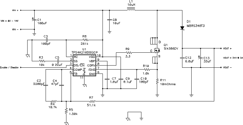 Figure 29. TPS40210-EP Design Example – 12-V to 24-V at 2 A
8.2.1 Design Requirements
Table 1. TPS40210-EP Design Example Specifications
| PARAMETER | TEST CONDITIONS | MIN | TYP | MAX | UNIT | |
|---|---|---|---|---|---|---|
| INPUT CHARACTERISTICS | ||||||
| VIN | Input voltage | 8 | 12 | 14 | V | |
| IIN | Input current | 4.4 | A | |||
| No load input current | 0.05 | |||||
| VIN(UVLO) | Input undervoltage lockout | 4.5 | V | |||
| OUTPUT CHARACTERISTICS | ||||||
| VOUT | Output voltage | 23.5 | 24.0 | 24.5 | V | |
| Line regulation | 1% | |||||
| Load regulation | 1% | |||||
| VOUT(ripple) | Output voltage ripple | 500 | mVPP | |||
| IOUT | Output current | 8 V ≤ VIN ≤ 14 V | 0.1 | 1 | 2.0 | A |
| IOCP | Output overcurrent inception point | 3.5 | ||||
| Transient response | ||||||
| ΔI | Load step | 1 | A | |||
| Load slew rate | 1 | A/μs | ||||
| Overshoot threshold voltage | 500 | mV | ||||
| Settling time | 5 | ms | ||||
| SYSTEM CHARACTERISTICS | ||||||
| ƒSW | Switching frequency | 600 | kHz | |||
| ηPK | Peak efficiency | VIN = 12 V | 95% | |||
| η | Full load efficiency | VIN = 12 V, IOUT = 2 A | 94% | |||
| TOP | Operating temperature range | 8 V ≤ VIN ≤ 14 V, IOUT ≤ 2 A | 25 | °C | ||
| MECHANICAL DIMENSIONS | ||||||
| W | Width | 1.5 | inch | |||
| L | Length | 1.5 | ||||
| h | Height | 0.5 | ||||
8.2.2 Detailed Design Procedure
8.2.2.1 Duty Cycle Estimation
The duty cycle of the main switching MOSFET is estimated using Equation 31 and Equation 32.


Using an estimated forward drop (VFD) of 0.5V for a schottky rectifier diode, the approximate duty cycle is 42.9% (minimum) to 67.3% (maximum).
8.2.2.2 Inductor Selection
The peak-to-peak ripple is chosen to be 30% of the maximum input current.

The minimum inductor size can be estimated using Equation 34.

The next higher standard inductor value of 10 μH is selected. The ripple current for nominal and minimum VIN is estimated by Equation 35 and Equation 36.


The worst case peak-to-peak ripple current occurs at 50% duty cycle (VIN = 12.25 V) and is estimated as 1.02 A. Worst case RMS current through the inductor is approximated by Equation 37.

The worst case RMS inductor current is 6.13 A. The peak inductor current is estimated by Equation 38.

A 10-μH inductor with a minimum RMS current rating of 6.13 A and minimum saturation current rating of 6.57 A must be selected. A TDK RLF12560T-100M-7R5 7.5-A 10-μH inductor is selected.
This inductor power dissipation is estimated by Equation 39.

The TDK RLF12560T-100M-7R5 12.4-mΩ DCR dissipates 466-mW of power.
8.2.2.3 Rectifier Diode Selection
A low forward voltage drop schottky diode is used as a rectifier diode to reduce its power dissipation and improve efficiency. Using 80% derating on VOUT for ringing on the switch node, the rectifier diode minimum reverse break-down voltage is given by Equation 40.

The diode must have reverse breakdown voltage greater than 30 V. The rectifier diode peak and average currents are estimated by Equation 41 and Equation 42.


The power dissipation in the diode is estimated by Equation 43.

For this design, the maximum power dissipation is estimated as 1 W. Reviewing 30-V and 40-V schottky diodes, the MBRS340T3, 40-V, 3-A diode in an SMC package is selected. This diode has a forward voltage drop of 0.48 V at 6 A, so the conduction power dissipation is approximately 960 mW, less than half its rated power dissipation.
8.2.2.4 Output Capacitor Selection
Output capacitors must be selected to meet the required output ripple and transient specifications.


A Panasonic EEEFC1V330P 35-V 33-μF, 120-mΩ bulk capacitor and a 6.8-μF ceramic capacitor are selected to provide the required capacitance and ESR at the switching frequency. The combined capacitance of 39.8 μF and ESR of 60 mΩ are used in compensation calculations.
8.2.2.5 Input Capacitor Selection
Since a boost converter has continuous input current, the input capacitor senses only the inductor ripple current. The input capacitor value can be calculated by Equation 46 and Equation 47 .


For this design to meet a maximum input ripple of 60mV (1/2% of VIN nominal), a minimum 7.1-μF input capacitor with ESR less than 29mΩ is needed. A 10-μF, X7R ceramic capacitor is selected.
8.2.2.6 Current Sense and Current Limit
The maximum allowable current sense resistor value is limited by both the current limit and sub-harmonic stability. These two limitations are given by Equation 48 and Equation 49.


With 10% margin on the current limit trip point (the 1.1 factor) and assuming a maximum gate drive current of 500 mA, the current limit requires a resistor less than 15.4 mΩ and stability requires a sense resistor less than 134 mΩ. A 10-mΩ resistor is selected. Approximately 2 mΩ of routing resistance is added in compensation calculations.
The power dissipation in RISNS is calculated by Equation 50.

At maximum duty cycle, this is 0.253 W.
8.2.2.7 Current Sense Filter
To remove switching noise from the current sense, an RC filter is placed between the current sense resistor and the ISNS pin. A resistor with a value between 1 kΩ and 5 kΩ is selected and a capacitor value is calculated by Equation 51.

For a 1-kΩ filter resistor, 71pF is calculated and a 100-pF capacitor is selected.
8.2.2.8 Switching MOSFET Selection
The TPS40210-EP drives a ground referenced N-channel FET. The RDS(on) and gate charge are estimated based on the desired efficiency target.

For a target of 95% efficiency with a 24-V Input voltage at 2 A, maximum power dissipation is limited to 2.526 W. The main power dissipating devices are the MOSFET, inductor, diode, current sense resistor and the integrated circuit, the TPS40210-EP.

This leaves 812 mW of power dissipation for the MOSFET. This can likely cause an SO-8 MOSFET to get too hot, so power dissipation is limited to 500 mW. Allowing half for conduction and half for switching losses, we can determine a target RDS(on) and QGS for the MOSFET by Equation 54 and Equation 55.

A target MOSFET gate-to-source charge of less than 13.0 nC is calculated to limit the switching losses to less than 250 mW.

A target MOSFET RDS(on) of 9.9 mΩ is calculated to limit the conduction losses to less than 250 mW. Reviewing 30-V and 40-V MOSFETs, an Si4386DY 9-mΩ MOSFET is selected. A gate resistor was added per Equation 30. The maximum gate charge at VGS= 8V for the Si4386DY is 33.2 nC, this implies RG = 3.3 Ω.
8.2.2.9 Feedback Divider Resistors
The primary feedback divider resistor (RFB) from VOUT to FB should be selected between 10 kΩ and 100 kΩ to maintain a balance between power dissipation and noise sensitivity. For a 24-V output a high feedback resistance is desirable to limit power dissipation so RFB = 51.1 kΩ is selected.

RBIAS = 1.50kΩ is selected.
8.2.2.10 Error Amplifier Compensation
Compensation selection can be done with aid of WEBENCH to select compensation components or with the aid of the average Spice model to simulate the open loop modulator and power stage gain. Alternatively the following procedure gives a good starting point.
While current mode control typically only requires Type II compensation, it is desirable to layout for Type III compensation to increase flexibility during design and development. Current mode control boost converters have higher gain with higher output impedance, so it is necessary to calculate the control loop gain at the maximum output impedance, estimated by Equation 57.

The transconductance of the TPS40210-EP current mode control can be estimated by Equation 58.

The maximum output impedance ZOUT, can be estimated by Equation 59.


At the desired crossover frequency (ƒL) of 30 kHz, ZOUT becomes 0.146 Ω.
The modulator gain at the desired cross-over can be estimated by Equation 61.

The feedback compensation network needs to be designed to provide an inverse gain at the cross-over frequency for unity loop gain. This sets the compensation mid-band gain at a value calculated in Equation 62.

To set the mid-band gain of the error amplifier to KCOMP use Equation 63.

R4 = 18.7 kΩ selected.
Place the zero at 1/10th of the desired cross-over frequency.

C2 = 2200 pF selected.
Place a high-frequency pole at about 5 times the desired cross-over frequency and less than one-half the unity gain bandwidth of the error amplifier:


C4 = 47 pF selected.
8.2.2.11 RC Oscillator
The RC oscillator calculation is given as shown in Equation 14 in the datasheet, substituting 100 for CT and 600 for ƒSW. For a 600-kHz switching frequency, a 100pF capacitor is selected and a 262-kΩ resistor is calculated (261-kΩ selected).
8.2.2.12 Soft-Start Capacitor
Since VDD > 8 V, the soft-start capacitor is selected by using Equation 67 to calculate the value.

For TSS = 12 ms, CSS = 240 nF. A 220-nF capacitor is selected.
8.2.2.13 Regulator Bypass
A regulator bypass (BP) capacitor of 1.0 μF is selected per the datasheet recommendation.
8.2.2.14 Bill of Materials
Table 2. Bill of Materials
| REFERENCE DESIGNATOR |
DESCRIPTION | SIZE | PART NUMBER |
MANUFAC- TURER |
|---|---|---|---|---|
| C1 | 100 μF, aluminum capacitor, SM, ± 20%, 35 V | 0.406 x 0.457 | EEEFC1V101P | Panasonic |
| C2 | 2200 pF, ceramic capacitor, 25 V, X7R, 20% | 0603 | Std | Std |
| C3 | 100 pF, ceramic capacitor, 16 V, C0G, 10% | 0603 | Std | Std |
| C4 | 47 pF, ceramic capacitor, 16V, X7R, 20% | 0603 | Std | Std |
| C5 | 0.22 μF, ceramic capacitor, 16 V, X7R, 20% | 0603 | Std | Std |
| C7 | 1.0 μF, ceramic capacitor, 16 V, X5R, 20% | 0603 | Std | Std |
| C8 | 10 μF, ceramic capacitor, 25 V, X7R, 20% | 0805 | C3225X7R1E106M | TDK |
| C9 | 0.1 μF, ceramic capacitor, 50 V, X7R, 20% | 0603 | Std | Std |
| C10 | 100 pF, ceramic capacitor, 16 V, X7R, 20% | 0603 | Std | Std |
| D1 | Schottky diode, 3 A, 40 V | SMC | MBRS340T3 | On Semi |
| L1 | 10 μH, inductor, SMT, 7.5 A, 12.4 mΩ | 0.325 x 0.318 inch | RLF12560T-100M-7R5 | TDK |
| Q1 | MOSFET, N-channel, 40 V, 14 A, 9mΩ | SO-8 | Si4840DY | Vishay |
| R3 | 10 kΩ, chip resistor, 1/16 W, 5% | 0603 | Std | Std |
| R4 | 18.7 kΩ, chip resistor, 1/16 W, 1% | 0603 | Std | Std |
| R5 | 1.5 kΩ, chip resistor, 1/16 W, 1% | 0603 | Std | Std |
| R6 | 261 kΩ, chip resistor, 1/16 W, 1% | 0603 | Std | Std |
| R7 | 51.1 kΩ, chip resistor, 1/16 W, 1% | 0603 | Std | Std |
| R9 | 3.3 Ω, chip resistor, 1/16 W, 5% | 0603 | Std | Std |
| R10 | 1.0 kΩ, chip resistor, 1/16 W, 5% | 0603 | Std | Std |
| R11 | 10 mΩ, chip resistor, 1/2 W, 2% | 1812 | Std | Std |
| U1 | IC, 4.5 V-52 V I/P, current mode boost controller | DGQ10 | TPS40210-EPDGQ | TI |
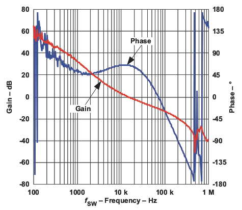
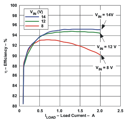
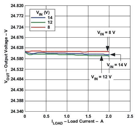
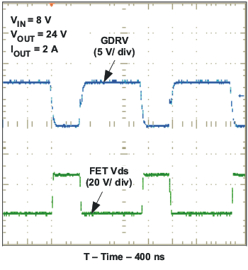
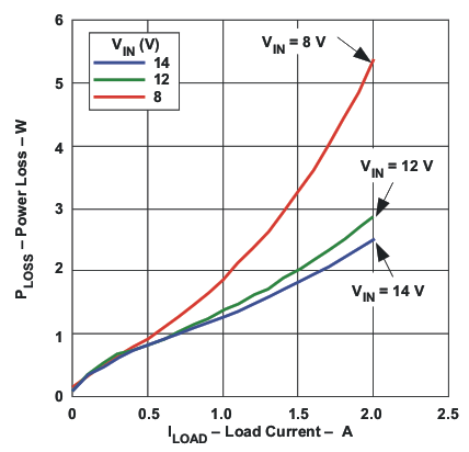
8.2.3 Application Curves
