SLUS772G March 2008 – June 2020 TPS40210 , TPS40211
PRODUCTION DATA
- 1 Features
- 2 Applications
- 3 Description
- 4 Revision History
- 5 Pin Configuration and Functions
- 6 Specifications
-
7 Detailed Description
- 7.1 Overview
- 7.2 Functional Block Diagram
- 7.3
Feature Description
- 7.3.1 Soft Start
- 7.3.2 BP Regulator
- 7.3.3 Shutdown (DIS/ EN Pin)
- 7.3.4 Minimum On-Time and Off-Time Considerations
- 7.3.5 Setting the Oscillator Frequency
- 7.3.6 Synchronizing the Oscillator
- 7.3.7 Current Sense and Overcurrent
- 7.3.8 Current Sense and Subharmonic Instability
- 7.3.9 Current Sense Filtering
- 7.3.10 Control Loop Considerations
- 7.3.11 Gate Drive Circuit
- 7.3.12 TPS40211
- 7.4 Device Functional Modes
-
8 Application and Implementation
- 8.1 Application Information
- 8.2
Typical Applications
- 8.2.1
12-V to 24-V Nonsynchronous Boost Regulator
- 8.2.1.1 Design Requirements
- 8.2.1.2
Detailed Design Procedure
- 8.2.1.2.1 Custom Design with WEBENCH Tools
- 8.2.1.2.2 Duty Cycle Estimation
- 8.2.1.2.3 Inductor Selection
- 8.2.1.2.4 Rectifier Diode Selection
- 8.2.1.2.5 Output Capacitor Selection
- 8.2.1.2.6 Input Capacitor Selection
- 8.2.1.2.7 Current Sense and Current Limit
- 8.2.1.2.8 Current Sense Filter
- 8.2.1.2.9 Switching MOSFET Selection
- 8.2.1.2.10 Feedback Divider Resistors
- 8.2.1.2.11 Error Amplifier Compensation
- 8.2.1.2.12 RC Oscillator
- 8.2.1.2.13 Soft-Start Capacitor
- 8.2.1.2.14 Regulator Bypass
- 8.2.1.2.15 Bill of Materials
- 8.2.1.3 Application Curves
- 8.2.2 12-V Input, 700-mA LED Driver, Up to 35-V LED String
- 8.2.1
12-V to 24-V Nonsynchronous Boost Regulator
- 9 Power Supply Recommendations
- 10Layout
- 11Device and Documentation Support
- 12Mechanical, Packaging, and Orderable Information
封装选项
请参考 PDF 数据表获取器件具体的封装图。
机械数据 (封装 | 引脚)
- DRC|10
- DGQ|10
散热焊盘机械数据 (封装 | 引脚)
订购信息
7.3.12 TPS40211
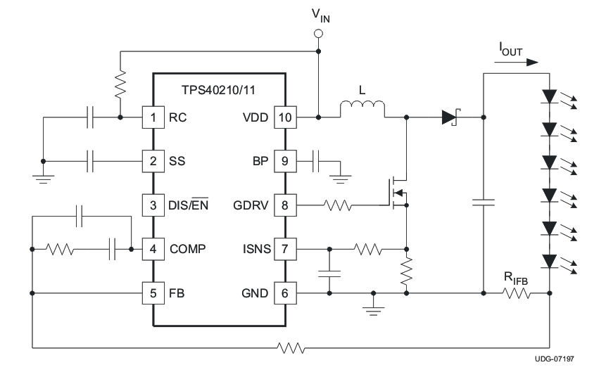
The only difference between the TPS40210 and the TPS40211 is the reference voltage that the error amplifier uses to regulate the output voltage. The TPS40211 uses a 260-mV reference and is intended for applications where the output is actually a current instead of a regulated voltage. A typical example of an application of this type is an LED driver. An example schematic is shown in Figure 7-10.
 Figure 7-10 Typical LED Drive Schematic
The current in the LED string is set by the choice of the resistor RISNS as shown in Equation 31.
Equation 31. 

where
- RIFB is the value of the current sense resistor for the LED string in Ω
- VFB is the reference voltage for the TPS40211 in V (0.260 V typ.)
- IOUT is the desired DC current in the LED string in A