SLUSAF8E July   2011  – January 2016 TPS40322

PRODUCTION DATA.  

  1. Features
  2. Applications
  3. Description
  4. Revision History
  5. Pin Configuration and Functions
  6. Specifications
    1. 6.1 Absolute Maximum Ratings
    2. 6.2 ESD Ratings
    3. 6.3 Recommended Operating Conditions
    4. 6.4 Thermal Information
    5. 6.5 Electrical Characteristics
    6. 6.6 Typical Characteristics
  7. Detailed Description
    1. 7.1 Overview
    2. 7.2 Functional Block Diagram
    3. 7.3 Feature Description
      1. 7.3.1  Voltage Reference
      2. 7.3.2  Output Voltage Setting
      3. 7.3.3  Input Voltage Feedforward
      4. 7.3.4  Current Sensing
      5. 7.3.5  Overcurrent Protection
      6. 7.3.6  Two-Phase Mode, Remote Sense Amplifier, and Current Sharing Loop
      7. 7.3.7  Start-Up and Shutdown
        1. 7.3.7.1 Start-Up Sequence
        2. 7.3.7.2 Prebiased Output Start-Up
        3. 7.3.7.3 Shutdown
      8. 7.3.8  Switching Frequency and Master or Slave Synchronization
      9. 7.3.9  Overvoltage and Undervoltage Fault Protection
      10. 7.3.10 Input Undervoltage Lockout (UVLO)
      11. 7.3.11 Power Good
      12. 7.3.12 Thermal Shutdown
      13. 7.3.13 Connection of Unused Pins
    4. 7.4 Device Functional Modes
  8. Applications and Implementation
    1. 8.1 Application Information
    2. 8.2 Typical Applications
      1. 8.2.1 Dual-Output Configuration from 12-V Nominal to 1.2-V and 1.8-V DC-to-DC Converter Using the TPS40322
        1. 8.2.1.1 Design Requirements
        2. 8.2.1.2 Detailed Design Procedure
          1. 8.2.1.2.1  Selecting a Switching Frequency
          2. 8.2.1.2.2  Inductor Selection (L1)
          3. 8.2.1.2.3  Output Capacitor Selection (C10 through C16)
          4. 8.2.1.2.4  Peak Current Rating of Inductor
          5. 8.2.1.2.5  Input Capacitor Selection (C3 through C6)
          6. 8.2.1.2.6  MOSFET Selection (Q1)
          7. 8.2.1.2.7  ILIM Resistor (R2)
          8. 8.2.1.2.8  Feedback Divider (R10, R14)
          9. 8.2.1.2.9  Compensation: (R11, R12, C17, C19, C21)
          10. 8.2.1.2.10 Boot-Strap Capacitor (C7)
          11. 8.2.1.2.11 General Device Components
            1. 8.2.1.2.11.1 Synchronization (SYNC Pin)
            2. 8.2.1.2.11.2 RT Resistor (R6)
            3. 8.2.1.2.11.3 Differential Amplifier Out (DIFFO Pin)
            4. 8.2.1.2.11.4 EN/SS Timing Capacitors (C8)
            5. 8.2.1.2.11.5 Power Good (PG1, PG2 Pins)
            6. 8.2.1.2.11.6 Phase Set (PHSET Pin)
            7. 8.2.1.2.11.7 UVLO Programming Resistors (R1 and R3)
            8. 8.2.1.2.11.8 VDD Bypass Capacitor (C2)
            9. 8.2.1.2.11.9 VBP6 Bypass Capacitor (C18)
        3. 8.2.1.3 Application Curves
      2. 8.2.2 Two-Phase, Single Output Configuration from 12-V nominal to 1.2-V DC-to-DC Converter Using the TPS40322
        1. 8.2.2.1 Design Requirements
        2. 8.2.2.2 Detailed Design Procedure
        3. 8.2.2.3 Application Curves
  9. Power Supply Recommendations
  10. 10Layout
    1. 10.1 Layout Guidelines
      1. 10.1.1 Power Stage
      2. 10.1.2 Device Peripheral
      3. 10.1.3 Thermal Pad Layout
    2. 10.2 Layout Example
    3. 10.3 Mounting and Thermal Profile Recommendation
  11. 11Device and Documentation Support
    1. 11.1 Device Support
      1. 11.1.1 Third-Party Products Disclaimer
      2. 11.1.2 Development Support
    2. 11.2 Documentation Support
      1. 11.2.1 Related Documentation
    3. 11.3 Community Resources
    4. 11.4 Trademarks
    5. 11.5 Electrostatic Discharge Caution
    6. 11.6 Glossary
  12. 12Mechanical, Packaging, and Orderable Information

封装选项

机械数据 (封装 | 引脚)
散热焊盘机械数据 (封装 | 引脚)
订购信息

5 Pin Configuration and Functions

RHB Package
32-Pin VQFN
Top View
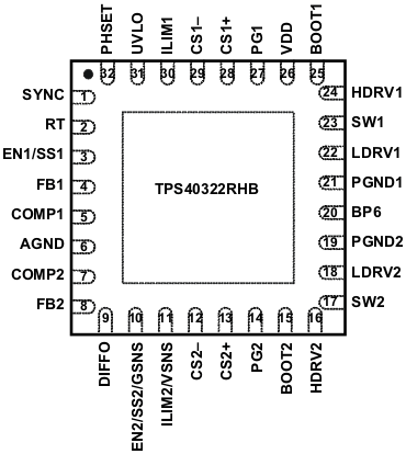
TPS40322 rhb_32_po_lusaf8.gif

NOTE:

In two-phase mode, the EN2/SS2/GSNS pin becomes the GSNS pin and the ILIM2/VSNS pin becomes the VSNS pin.
The two channels are identical unless specified otherwise.
The following naming conventions are used to better describe the functions. For example, COMPx refers to COMP1 and COMP2, FBx refers to FB1 and FB2.

Pin Functions

PIN I/O DESCRIPTION
NAME PIN
AGND 6 Low noise ground connection to the controller.
BOOT1 25 I BOOT1 provides a bootstrapped supply for the high-side FET driver for channel 1 (CH1). Connect a capacitor (0.1 μF typical) from BOOT1 to SW1 pin.
BOOT2 15 I BOOT2 provides a bootstrapped supply for the high-side FET driver for channel 2 (CH2). Connect a capacitor (0.1 μF typical) from BOOT2 to SW2 pin.
BP6 20 O Output bypass for the internal regulator. Connect a low ESR bypass ceramic capacitor with a value of
3.3 μF or greater from this pin to the power ground plane.
COMP1 5 O Output of the error amplifier 1 and connection node for loop feedback components.
COMP2 7 O Output of the error amplifier 2 and connection node for loop feedback components.
CS1– 29 I Negative terminal of current sense amplifier for CH1
CS1+ 28 I Positive terminal of current sense amplifier for CH1
CS2– 12 I Negative terminal of current sense amplifier for CH2
CS2+ 13 I Positive terminal of current sense amplifier for CH2
DIFFO 9 O Output of the differential amplifier. When the device is configured for dual channel mode, the DIFFO pin must be either floating or tied to BP6
EN1/SS1 3 I Logic level input which starts or stops CH1. Letting this pin float turns CH1 on. Pulling this pin low disables CH1. This is also the soft-start programming pin. A capacitor connected from this pin to AGND programs the soft-start time. The capacitor is charged with an internal current source of 10 μA. The resulting voltage ramp of this pin is also used as a second non-inverting input to the error amplifier 1 after a 0.8 V (typical) level shift downwards.
EN2/SS2/GSNS 10 I Logic level input which starts or stops CH2. Letting this pin float turns CH2 on. Pulling this pin low disables CH2. This is also the soft-start programming pin. A capacitor connected from this pin to AGND programs the soft-start time. The capacitor is charged with an internal current source of 10 μA. The resulting voltage ramp of this pin is also used as a second non-inverting input to the error amplifier 2 after a 0.8 V (typical) level shift downwards. In two-phase mode, this pin becomes GSNS as the negative terminal of a remote sense amplifier.
FB1 4 I Inverting input to the error amplifier. During normal operation, the voltage on this pin is equal to the internal reference voltage.
FB2 8 I Inverting input to the error amplifier. During normal operation, the voltage on this pin is equal to the internal reference voltage. Connecting the FB2 pin to the BP6 pin enables two-phase mode and disables the error amplifier 2.
HDRV1 24 O Bootstrapped gate drive output for the high-side N-channel MOSFET for CH1. A 2-Ω resistor is recommended for a noisy environment.
HDRV2 16 O Bootstrapped gate drive output for the high-side N-channel MOSFET for CH2. A 2-Ω resistor is recommended for a noisy environment.
ILIM1 30 I Used to set the overcurrent limit for CH1 with 10 μA of current flowing through a resistor from this pin to AGND.
ILIM2/VSNS 11 I Used to set the overcurrent limit for CH2 with 10 μA of current flowing through a resistor from this pin to AGND. In two-phase mode, this pin becomes VSNS as the positive terminal of a remote sense amplifier.
LDRV1 22 O Gate drive output for the low-side synchronous rectifier (SR) N-channel MOSFET for CH1.
LDRV2 18 O Gate drive output for the low-side synchronous rectifier (SR) N-channel MOSFET for CH2.
PG1 27 O Open drain power good indicator for CH1 output voltage.
PG2 14 O Open drain power good indicator for CH2 output voltage.
PGND1 21 Power ground 1. Separate power ground for CH1 and CH2 in the PCB layout could potentially reduce channel to channel interference.
PGND2 19 Power ground 2. Separate power ground for CH1 and CH2 in the PCB layout could potentially reduce channel to channel interference.
PHSET 32 I Used to set master or slave mode and phase angles. The master emits a 50% duty clock to the slave. The slave synchronizes to the external clock and select the phase shift angle.
RT 2 I Connect a resistor from this pin to AGND to set the oscillator frequency.
SW1 23 I Connect to the switched node on converter CH1. It is the return for the CH 1 high-side gate driver.
SW2 17 I Connect to the switched node on converter CH2. It is the return for the CH 2 high-side gate driver.
SYNC 1 I/O In master mode, a 2x free running frequency clock is sent out on SYNC pin. In slave mode, sync to an external clock which is ±20% of the free running MASTER_CLOCK frequency. The MASTER_CLOCK frequency is 2x of the free running frequency (set by RT) and operates at 50% duty cycle. When not being used, SYNC must be left floating.
UVLO 31 I A resistor divider from VIN determines the input voltage that the controller starts.
VDD 26 I Power input to the controller. A low ESR bypass ceramic capacitor of 0.1 μF or greater must be connected closely from this pin to AGND.