-
TPS4306x 低静态电流同步升压 DC-DC 控制器,支持宽 VIN 范围
- 1 特性
- 2 应用
- 3 说明
- 4 简化电路原理图
- 5 修订历史记录
- 6 Pin Configuration and Functions
- 7 Specifications
-
8 Detailed Description
- 8.1 Overview
- 8.2 Functional Block Diagram
- 8.3
Feature Description
- 8.3.1 Switching Frequency
- 8.3.2 Low-Dropout Regulator
- 8.3.3 Input Undervoltage (UV)
- 8.3.4 Enable and Adjustable UVLO
- 8.3.5 Voltage Reference and Setting Output Voltage
- 8.3.6 Minimum On-Time and Pulse Skipping
- 8.3.7 Zero-Cross Detection and Duty Cycle
- 8.3.8 Minimum Off-Time and Maximum Duty Cycle
- 8.3.9 Soft-Start
- 8.3.10 Power Good
- 8.3.11 Overvoltage Protection (OVP)
- 8.3.12 OVP and Current Sense Resistor Selection
- 8.3.13 Gate Drivers
- 8.3.14 Thermal Shutdown
- 8.4 Device Functional Modes
-
9 Application and Implementation
- 9.1 Application Information
- 9.2
Typical Applications
- 9.2.1
Synchronous Boost Converter Typical Application Using TPS43061
- 9.2.1.1 Design Requirements
- 9.2.1.2
Detailed Design Procedure
- 9.2.1.2.1 Selecting the Switching Frequency
- 9.2.1.2.2 Inductor Selection
- 9.2.1.2.3 Selecting the Current Sense Resistor
- 9.2.1.2.4 Output Capacitor Selection
- 9.2.1.2.5 MOSFET Selection - NexFET Power Block
- 9.2.1.2.6 Bootstrap Capacitor Selection
- 9.2.1.2.7 VCC Capacitor
- 9.2.1.2.8 Input Capacitor
- 9.2.1.2.9 Output Voltage and Feedback Resistors Selection
- 9.2.1.2.10 Setting the Soft-Start Time
- 9.2.1.2.11 UVLO Set Point
- 9.2.1.2.12 Power Good Resistor Selection
- 9.2.1.2.13 Control Loop Compensation
- 9.2.1.2.14 DCM, Pulse-Skip Mode, and No-Load Input Current
- 9.2.1.3 Application Curves
- 9.2.2 High-Efficiency 40-V Synchronous Boost Converter Typical Application Using TPS43060
- 9.2.1
Synchronous Boost Converter Typical Application Using TPS43061
- 10Power Supply Recommendations
- 11Layout
- 12器件和文档支持
- 13机械、封装和可订购信息
- 重要声明
DATA SHEET
TPS4306x 低静态电流同步升压 DC-DC 控制器,支持宽 VIN 范围
本资源的原文使用英文撰写。 为方便起见,TI 提供了译文;由于翻译过程中可能使用了自动化工具,TI 不保证译文的准确性。 为确认准确性,请务必访问 ti.com 参考最新的英文版本(控制文档)。
1 特性
- 58V 最大输出电压
- VIN 范围:4.5V 至 38V(绝对最大值为 40V)
- TPS43060:针对标准阈值 MOSFET 优化的 7.5V 栅极驱动器
- TPS43061:针对低 Qg 优化的 5.5V 栅极驱动器 NexFET™功率 MOSFET
- 支持内部斜率补偿的电流模式控制
- 可调频率范围:50kHz 至 1MHz
- 同步外部时钟功能
- 可调软启动时间
- 电感器直流电阻 (DCR) 或电阻器电流感测
- 输出电压电源正常指示器
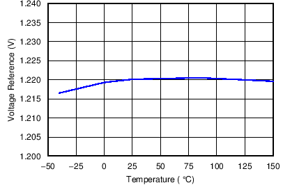
- ±0.8% 反馈基准电压
- 5µA 关断电源电流
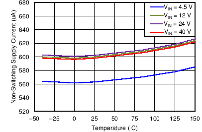
- 600µA 静态工作电流
- 集成引导加载二极管 (TPS43061)
- 逐周期电流限制和热关断
- 可调节的欠压闭锁 (UVLO) 和输出过压保护
- 小型 16 引脚 WQFN (3mm × 3mm) 封装,带有 PowerPAD™
- 运行 TJ范围:–40°C 至 150°C
2 应用
- 用于 PC 的 Thunderbolt 端口
- 汽车电源系统
- 同步回扫
- 氮化镓 (GaN) 射频 (RF) 功率放大器
- 平板笔记本附件
- 电池供电系统
- 5V、12V 和 24V 直流总线电源系统
3 说明
TPS43060 和 TPS43061 是低 IQ 电流模式同步升压控制器,支持 4.5V 至 38V(绝对最大值为 40V)的宽输入电压范围和高达 58V 的升压输出范围。同步整流功能可为高电流 应用实现高效率,无损电感直流电阻 (DCR) 感测功能可进一步提升效率。该器件产生的功率损耗较低,并且采用带 PowerPAD™的 3mm × 3mm WQFN-16 封装,可以在扩展级温度范围(-40°C 至 150°C)内支持高功率密度且高可靠性的升压转换器解决方案。
TPS43060 含有一个 7.5V 栅极驱动电源,适合驱动各种 MOSFET。TPS43061 具有一个 5.5V 栅极驱动电源,驱动强度针对低 Qg NexFET 功率 MOSFET 进行了优化。另外,TPS43061 为高侧栅极驱动器提供了一个集成型自举二极管,从而减少了外部部件数量。
器件信息(1)
| 器件型号 | 封装 | 封装尺寸(标称值) |
|---|---|---|
| TPS43060 | RTE (16) | 3.00mm × 3.00mm |
| TPS43061 |
- 要了解所有可用封装,请见数据表末尾的可订购米6体育平台手机版_好二三四附录。
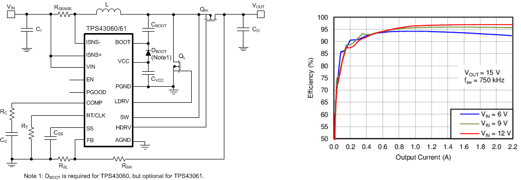
4 简化电路原理图
5 修订历史记录
Changes from C Revision (September 2013) to D Revision
- 已添加处理额定值表,特性 描述部分,器件功能模式,应用和实施部分,电源相关建议部分,布局部分,器件和文档支持部分以及机械、封装和可订购信息部分Go
Changes from B Revision (August 2013) to C Revision
- Changed Equation 3Go
- Deleted sections Layout Considerations and Thermal ConsiderationsGo
- Changed Equation 13 from Dmin to (1-Dmax), 60% to (1-60%) and 2.4 MHz to 1.6 MHzGo
- Changed 2 MHz to 1.6 MHz in para below Equation 13Go
- Changed in Equation 28 – DS(on)LS to DS(on)HSGo
- Changed in Equation 29 – from (60 ns + 65 ns) to (65 ns _65 ns)Go
- Changed in paragraph above Equation 37 - 1.93 kHz to 0.97 kHzGo
- Changed in Equation 38 – from 1.93 kHz to 0.97 kHzGo
- Changed in paragraph above Equation 43 – 7.44 kΩ to 7.45 kΩGo
- Changed in Equation 43 – 21 µF to 22 µF, 20 mΩ to 10 mΩ, 19.3 kHz to 14.5 kHz, = 7.44 to = 7.45, and deleted 3/40 factor from denominatorGo
Changes from A Revision (December 2012) to B Revision
Changes from * Revision (December 2012) to A Revision
- 已将器件从“预览”更改为“量产”Go
6 Pin Configuration and Functions
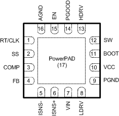
WQFN-16 PACKAGE
(TOP VIEW)
Pin Functions
| PIN | DESCRIPTION | |
|---|---|---|
| NAME | NO. | |
| RT/CLK | 1 | Resistor timing and external clock. An external resistor from this pin to the AGND pin programs the switching frequency between 50 kHz and 1 MHz. Driving the pin with an external clock between 300 kHz to 1 MHz synchronizes the switching frequency to the external clock. |
| SS | 2 | Soft-start programming pin. A capacitor between the SS pin and AGND pin sets soft-start time. |
| COMP | 3 | Output of the internal transconductance error amplifier. The feedback loop compensation network is connected from this pin to AGND. |
| FB | 4 | Error amplifier input and feedback pin for voltage regulation. Connect this pin to the center tap of a resistor divider to set the output voltage. |
| ISNS– | 5 | Inductor current sense comparator inverting input pin. This pin is normally connected to the inductor side of the current sense resistor. |
| ISNS+ | 6 | Inductor current sense comparator non-inverting input pin. This pin is normally connected to the VIN side of the current sense resistor. |
| VIN | 7 | The input supply pin to the IC. Connect VIN to a supply voltage between 4.5 and 38 V. It is acceptable for the voltage on the VIN pin to be different from the boost power stage input, ISNS+, and ISNS– pins. |
| LDRV | 8 | Low-side gate driver output. Connect this pin to the gate of the low-side N-channel MOSFET. When VIN bias is removed, an internal 200-kΩ resistor pulls LDRV to PGND. |
| PGND | 9 | Power ground of the IC. Connect this pin to the source of the low-side MOSFET. PGND should be connected to AGND via a single point on the PCB. |
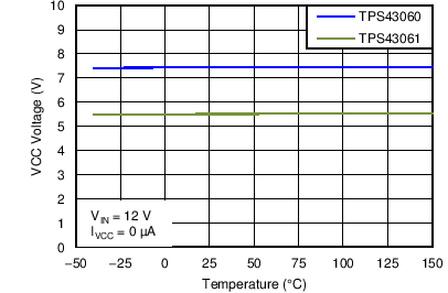
| VCC | 10 | Output of an internal LDO and power supply for internal control circuits and gate drivers. VCC is typically 7.5 V for the TPS43060 and 5.5 V for the TPS43061. Connect a low-ESR ceramic capacitor from this pin to PGND. TI recommends a capacitance range from 0.47 to 10 µF. |
| BOOT | 11 | Bootstrap capacitor node for high-side MOSFET gate driver. Connect the bootstrap capacitor from this pin to the SW pin. For the TPS43060, also connect a bootstrap diode from VCC to BOOT. |
| SW | 12 | Switching node of the boost converter. Connect this pin to the junction of the drain of the low-side MOSFET, the source of high-side synchronous MOSFET, and the inductor. |
| HDRV | 13 | High-side gate driver output. Connect this pin to the gate of the high-side synchronous rectifier MOSFET. When VIN bias is removed, this pin is connected to SW through an internal 200-kΩ resistor. |
| PGOOD | 14 | Power good indicator. This pin is an open-drain output. TI recommends a 10-kΩ pullup resistor between PGOOD and VCC or an external logic supply pin. |
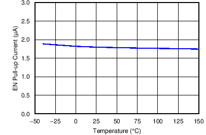
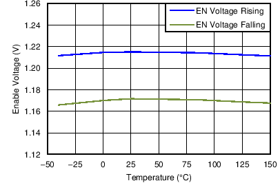
| EN | 15 | Enable pin with internal pullup current source. Floating this pin will enable the IC. Pull below 1.2 V to enter low current standby mode. Pull below 0.4 V to enter shutdown mode. The EN pin can be used to implement adjustable UVLO using two resistors. |
| AGND | 16 | Analog signal ground of the IC. AGND should be connected to PGND at a single point on the PCB. |
| PowerPAD | 17 | The PowerPAD should be connected to AGND. If possible, use thermal vias to connect to an internal ground plane for improved power dissipation. |
7 Specifications
7.1 Absolute Maximum Ratings
over operating free-air temperature (unless otherwise noted)| MIN | MAX | UNIT | ||
|---|---|---|---|---|
| Voltage | Input: VIN, EN, ISNS+, ISNS– | –0.3 | 40 | V |
| DC voltage: SW | –0.6 | 60 | V | |
| Transient voltage (10 ns max): SW | –2 | 60 | V | |
| FB, RT/CLK, COMP, SS | –0.3 | 3.6 | V | |
| BOOT, HDRV voltage with respect to ground | 65 | V | ||
| BOOT, HDRV voltage with respect to SW pin | 8 | V | ||
| VCC, PGOOD, LDRV | –0.3 | 8 | V | |
| Operating junction temperature | –40 | 150 | °C | |
7.2 Handling Ratings
| MIN | MAX | UNIT | |||
|---|---|---|---|---|---|
| Tstg | Storage temperature range | –65 | 150 | °C | |
| V(ESD) | Electrostatic discharge | Human body model (HBM), per ANSI/ESDA/JEDEC JS-001, all pins(1) | –2000 | 2000 | V |
| Charged device model (CDM), per JEDEC specification JESD22-C101, all pins(2) | –500 | 500 | |||
(1) JEDEC document JEP155 states that 500-V HBM allows safe manufacturing with a standard ESD control process.
(2) JEDEC document JEP157 states that 250-V CDM allows safe manufacturing with a standard ESD control process.
7.3 Recommended Operating Conditions
over operating free-air temperature range (unless otherwise noted)| MIN | NOM | MAX | UNIT | ||
|---|---|---|---|---|---|
| VIN | Input voltage range | 4.5 | 38 | V | |
| VOUT | Output voltage range | VIN | 58 | V | |
| VEN | EN voltage range | 0 | 38 | V | |
| VCLK | External switching frequency logic input range | 0 | 3.6 | V | |
| TJ | Operating junction temperature | –40 | 150 | °C | |
7.4 Thermal Characteristics
over operating free-air temperature range (unless otherwise noted)| THERMAL METRIC (1) | WQFN (16-PINS) |
UNIT | |
|---|---|---|---|
| RθJA | Junction-to-ambient thermal resistance | 65.7 | °C/W |
| RθJC(top) | Junction-to-case (top) thermal resistance | 42.3 | |
| RθJB | Junction-to-board thermal resistance | 18 | |
| ψJT | Junction-to-top characterization parameter | 0.9 | |
| ψJB | Junction-to-board characterization parameter | 17.9 | |
| RθJC(bot) | Junction-to-case (bottom) thermal resistance | 22.7 | |
(1) For more information about traditional and new thermal metrics, see the IC Package Thermal Metrics application report, SPRA953.
7.5 Electrical Characteristics
VIN = 4.5 to 38 V, TJ = –40ºC to 150ºC, unless otherwise noted. Typical values are at TA = 25ºC7.6 Typical Characteristics
VIN = 12 V, ƒSW = 500 kHz, TA = 25ºC (unless otherwise noted)
