ZHCSAP1D December 2012 – September 2014 TPS43060 , TPS43061
PRODUCTION DATA.
- 1 特性
- 2 应用
- 3 说明
- 4 简化电路原理图
- 5 修订历史记录
- 6 Pin Configuration and Functions
- 7 Specifications
-
8 Detailed Description
- 8.1 Overview
- 8.2 Functional Block Diagram
- 8.3
Feature Description
- 8.3.1 Switching Frequency
- 8.3.2 Low-Dropout Regulator
- 8.3.3 Input Undervoltage (UV)
- 8.3.4 Enable and Adjustable UVLO
- 8.3.5 Voltage Reference and Setting Output Voltage
- 8.3.6 Minimum On-Time and Pulse Skipping
- 8.3.7 Zero-Cross Detection and Duty Cycle
- 8.3.8 Minimum Off-Time and Maximum Duty Cycle
- 8.3.9 Soft-Start
- 8.3.10 Power Good
- 8.3.11 Overvoltage Protection (OVP)
- 8.3.12 OVP and Current Sense Resistor Selection
- 8.3.13 Gate Drivers
- 8.3.14 Thermal Shutdown
- 8.4 Device Functional Modes
-
9 Application and Implementation
- 9.1 Application Information
- 9.2
Typical Applications
- 9.2.1
Synchronous Boost Converter Typical Application Using TPS43061
- 9.2.1.1 Design Requirements
- 9.2.1.2
Detailed Design Procedure
- 9.2.1.2.1 Selecting the Switching Frequency
- 9.2.1.2.2 Inductor Selection
- 9.2.1.2.3 Selecting the Current Sense Resistor
- 9.2.1.2.4 Output Capacitor Selection
- 9.2.1.2.5 MOSFET Selection - NexFET Power Block
- 9.2.1.2.6 Bootstrap Capacitor Selection
- 9.2.1.2.7 VCC Capacitor
- 9.2.1.2.8 Input Capacitor
- 9.2.1.2.9 Output Voltage and Feedback Resistors Selection
- 9.2.1.2.10 Setting the Soft-Start Time
- 9.2.1.2.11 UVLO Set Point
- 9.2.1.2.12 Power Good Resistor Selection
- 9.2.1.2.13 Control Loop Compensation
- 9.2.1.2.14 DCM, Pulse-Skip Mode, and No-Load Input Current
- 9.2.1.3 Application Curves
- 9.2.2 High-Efficiency 40-V Synchronous Boost Converter Typical Application Using TPS43060
- 9.2.1
Synchronous Boost Converter Typical Application Using TPS43061
- 10Power Supply Recommendations
- 11Layout
- 12器件和文档支持
- 13机械、封装和可订购信息
7 Specifications
7.1 Absolute Maximum Ratings
over operating free-air temperature (unless otherwise noted)| MIN | MAX | UNIT | ||
|---|---|---|---|---|
| Voltage | Input: VIN, EN, ISNS+, ISNS– | –0.3 | 40 | V |
| DC voltage: SW | –0.6 | 60 | V | |
| Transient voltage (10 ns max): SW | –2 | 60 | V | |
| FB, RT/CLK, COMP, SS | –0.3 | 3.6 | V | |
| BOOT, HDRV voltage with respect to ground | 65 | V | ||
| BOOT, HDRV voltage with respect to SW pin | 8 | V | ||
| VCC, PGOOD, LDRV | –0.3 | 8 | V | |
| Operating junction temperature | –40 | 150 | °C | |
7.2 Handling Ratings
| MIN | MAX | UNIT | |||
|---|---|---|---|---|---|
| Tstg | Storage temperature range | –65 | 150 | °C | |
| V(ESD) | Electrostatic discharge | Human body model (HBM), per ANSI/ESDA/JEDEC JS-001, all pins(1) | –2000 | 2000 | V |
| Charged device model (CDM), per JEDEC specification JESD22-C101, all pins(2) | –500 | 500 | |||
(1) JEDEC document JEP155 states that 500-V HBM allows safe manufacturing with a standard ESD control process.
(2) JEDEC document JEP157 states that 250-V CDM allows safe manufacturing with a standard ESD control process.
7.3 Recommended Operating Conditions
over operating free-air temperature range (unless otherwise noted)| MIN | NOM | MAX | UNIT | ||
|---|---|---|---|---|---|
| VIN | Input voltage range | 4.5 | 38 | V | |
| VOUT | Output voltage range | VIN | 58 | V | |
| VEN | EN voltage range | 0 | 38 | V | |
| VCLK | External switching frequency logic input range | 0 | 3.6 | V | |
| TJ | Operating junction temperature | –40 | 150 | °C | |
7.4 Thermal Characteristics
over operating free-air temperature range (unless otherwise noted)| THERMAL METRIC (1) | WQFN (16-PINS) |
UNIT | |
|---|---|---|---|
| RθJA | Junction-to-ambient thermal resistance | 65.7 | °C/W |
| RθJC(top) | Junction-to-case (top) thermal resistance | 42.3 | |
| RθJB | Junction-to-board thermal resistance | 18 | |
| ψJT | Junction-to-top characterization parameter | 0.9 | |
| ψJB | Junction-to-board characterization parameter | 17.9 | |
| RθJC(bot) | Junction-to-case (bottom) thermal resistance | 22.7 | |
(1) For more information about traditional and new thermal metrics, see the IC Package Thermal Metrics application report, SPRA953.
7.5 Electrical Characteristics
VIN = 4.5 to 38 V, TJ = –40ºC to 150ºC, unless otherwise noted. Typical values are at TA = 25ºC7.6 Typical Characteristics
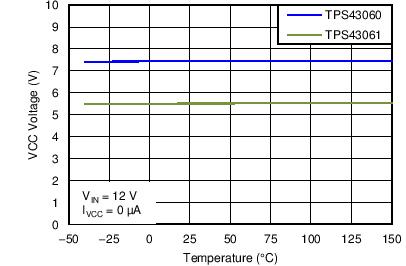
VIN = 12 V, ƒSW = 500 kHz, TA = 25ºC (unless otherwise noted)
