ZHCSET1B December   2015  – March 2018 TPS4H000-Q1

PRODUCTION DATA.  

  1. 特性
  2. 应用
  3. 说明
    1.     Device Images
      1.      典型应用原理图
      2.      驱动具有可调节电流限制的电容性负载
  4. 修订历史记录
  5. Device Comparison Table
  6. Pin Configuration and Functions
    1.     Pin Functions
  7. Specifications
    1. 7.1 Absolute Maximum Ratings
    2. 7.2 ESD Ratings
    3. 7.3 Recommended Operating Conditions
    4. 7.4 Thermal Information
    5. 7.5 Electrical Characteristics
    6. 7.6 Switching Characteristics
    7. 7.7 Typical Characteristics
  8. Detailed Description
    1. 8.1 Overview
    2. 8.2 Functional Block Diagram
    3. 8.3 Feature Description
      1. 8.3.1 Pin Current and Voltage Conventions
      2. 8.3.2 Accurate Current Sense
      3. 8.3.3 Adjustable Current Limit
      4. 8.3.4 Inductive-Load Switching-Off Clamp
      5. 8.3.5 Fault Detection and Reporting
        1. 8.3.5.1 Diagnostic Enable Function
        2. 8.3.5.2 Multiplexing of Current Sense
        3. 8.3.5.3 Fault Table
        4. 8.3.5.4 STx and FAULT Reporting
      6. 8.3.6 Full Diagnostics
        1. 8.3.6.1 Short-to-GND and Overload Detection
        2. 8.3.6.2 Open-Load Detection
          1. 8.3.6.2.1 Channel On
          2. 8.3.6.2.2 Channel Off
        3. 8.3.6.3 Short-to-Battery Detection
        4. 8.3.6.4 Reverse Polarity Detection
        5. 8.3.6.5 Thermal Fault Detection
          1. 8.3.6.5.1 Thermal Shutdown
      7. 8.3.7 Full Protections
        1. 8.3.7.1 UVLO Protection
        2. 8.3.7.2 Loss-of-GND Protection
        3. 8.3.7.3 Protection for Loss of Power Supply
        4. 8.3.7.4 Reverse-Current Protection
        5. 8.3.7.5 MCU I/O Protection
    4. 8.4 Device Functional Modes
      1. 8.4.1 Working Modes
  9. Application and Implementation
    1. 9.1 Application Information
    2. 9.2 Typical Application
      1. 9.2.1 Design Requirements
      2. 9.2.2 Detailed Design Procedure
      3. 9.2.3 Application Curves
  10. 10Power Supply Recommendations
  11. 11Layout
    1. 11.1 Layout Guidelines
    2. 11.2 Layout Examples
      1. 11.2.1 Without a GND Network
      2. 11.2.2 With a GND Network
  12. 12器件和文档支持
    1. 12.1 接收文档更新通知
    2. 12.2 社区资源
    3. 12.3 商标
    4. 12.4 静电放电警告
    5. 12.5 Glossary
  13. 13机械、封装和可订购信息

封装选项

机械数据 (封装 | 引脚)
散热焊盘机械数据 (封装 | 引脚)
订购信息

Application Curves

Figure 38 shows a test example of soft-start when driving a big capacitive load. Figure 39 shows an expanded waveform of the output current.
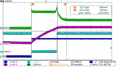
TPS4H000-Q1 app-curv1_SLVSD73.gif
Load current = 0.2 A CH2 = FAULT INx = ↑
Current limit = 0.5 A CH3 = output voltage CH1 = INx
CL = 2.3 mF CH4 = output current VS = 12 V
Figure 38. Driving a Capacitive Load
TPS4H000-Q1 app-curv2_SLVSD73.gif
Load current = 0.2 A CH2 = FAULT INx = ↑
Current limit = 0.5 A CH3 = output voltage CH1 = INx
CL = 2.3 mF CH4 = output current VVS = 12 V
Figure 39. Driving a Capacitive Load, Expanded Waveform

Figure 40 shows a test example of PWM-mode driving. Figure 41 shows the expanded waveform of the rising edge. Figure 42 shows the expanded waveform of the falling edge.

TPS4H000-Q1 app-curv3_SLVSD73.gif
INx = 200-Hz PWM, 50% duty cycle CH2 = CS voltage
VVS = 13.5 V CH3 = output voltage
CH1 = INx signal CH4 = output current
Figure 40. PWM Signal Driving
TPS4H000-Q1 app-curv5_SLVSD73.gif
INx = 200-Hz PWM, 50% duty cycle CH2 = CS voltage
VVS = 13.5 V CH3 = output voltage
CH1 = INx signal CH4 = output current
Figure 42. Expanded Waveform of Falling Edge
TPS4H000-Q1 app-curv4_SLVSD73.gif
INx = 200-Hz PWM, 50% duty cycle CH2 = CS voltage
VVS = 13.5 V CH3 = output voltage
CH1 = INx signal CH4 = output current
Figure 41. Expanded Waveform of Rising Edge