ZHCSB50K December 2012 – May 2019 TPS50301-HT
PRODUCTION DATA.
- 1 特性
- 2 应用
- 3 说明
- 4 修订历史记录
- 5 说明 (续)
- 6 Pin Configuration and Functions
- 7 Specifications
-
8 Detailed Description
- 8.1 Overview
- 8.2 Functional Block Diagram
- 8.3
Feature Description
- 8.3.1 VIN and Power VIN Pins (VIN and PVIN)
- 8.3.2 PVIN vs Frequency
- 8.3.3 Voltage Reference
- 8.3.4 Adjusting the Output Voltage
- 8.3.5 Maximum Duty Cycle Limit
- 8.3.6 PVIN vs Frequency
- 8.3.7 Safe Start-Up into Prebiased Outputs
- 8.3.8 Error Amplifier
- 8.3.9 Slope Compensation
- 8.3.10 Enable and Adjust UVLO
- 8.3.11 Adjustable Switching Frequency and Synchronization (SYNC)
- 8.3.12 Slow Start (SS/TR)
- 8.3.13 Power Good (PWRGD)
- 8.3.14 Bootstrap Voltage (BOOT) and Low Dropout Operation
- 8.3.15 Sequencing (SS/TR)
- 8.3.16 Output Overvoltage Protection (OVP)
- 8.3.17 Overcurrent Protection
- 8.3.18 TPS50301-HT Thermal Shutdown
- 8.3.19 Turn-On Behavior
- 8.3.20 Small Signal Model for Loop Response
- 8.3.21 Simple Small Signal Model for Peak Current Mode Control
- 8.3.22 Small Signal Model for Frequency Compensation
- 8.4 Device Functional Modes
-
9 Application and Implementation
- 9.1 Application Information
- 9.2
Typical Application
- 9.2.1 Design Requirements
- 9.2.2
Detailed Design Procedure
- 9.2.2.1 Custom Design With WEBENCH® Tools
- 9.2.2.2 Operating Frequency
- 9.2.2.3 Output Inductor Selection
- 9.2.2.4 Output Capacitor Selection
- 9.2.2.5 Input Capacitor Selection
- 9.2.2.6 Slow Start Capacitor Selection
- 9.2.2.7 Bootstrap Capacitor Selection
- 9.2.2.8 Undervoltage Lockout (UVLO) Set Point
- 9.2.2.9 Output Voltage Feedback Resistor Selection
- 9.2.2.10 Compensation Component Selection
- 9.2.3 Parallel Operation
- 9.2.4 Application Curve
- 10Power Supply Recommendations
- 11Layout
- 12器件和文档支持
- 13机械、封装和可订购信息
7.6 Dissipation Ratings
See (1)(2)(3)(4)(5)| PACKAGE | RθJA THERMAL IMPEDANCE,
JUNCTION TO AMBIENT |
RθJC THERMAL IMPEDANCE,
JUNCTION TO CASE (THERMAL PAD) |
RθJB THERMAL IMPEDANCE,
JUNCTION TO BOARD |
|---|---|---|---|
| HKH | 39.9°C/W | 0.52°C/W | 43.1°C/W |
(1) Maximum power dissipation may be limited by overcurrent protection
(2) Power rating at a specific ambient temperature, TA, should be determined with a junction temperature of 150°C. This is the point where distortion starts to substantially increase. Thermal management of the PCB should strive to keep the junction temperature at or below 150°C for best performance and long-term reliability. See power dissipation estimate in Application and Implementation for more information.
(3) Test board conditions:
(4) For information on thermal characteristics, see SPRA953.
(5) Use polyimide PCB and thermal management to ensure operation below maximum TJ operation.

A. See data sheet for absolute maximum and minimum recommended operating conditions.
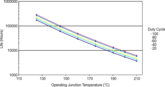
B. Silicon operating life design goal is 10 years at 125°C junction temperature (does not include package interconnect life).
C. The predicted operating lifetime versus junction temperature is based on reliability modeling using electromigration as the dominant failure mechanism affecting device wearout for the specific device process and design characteristics.
D. This device is rated for 1000 hours of continuous operation at maximum rated temperature at 210°C.
Figure 1. 3-A Continuous Current Estimated Device Life