ZHCSHX8D September   2017  – October 2019 TPS50601A-SP

PRODUCTION DATA.  

  1. 特性
    1.     VIN = PVIN = 5V 条件下的效率
  2. 应用
  3. 说明
  4. 修订历史记录
  5. Pin Configuration and Functions
    1.     Pin Functions
  6. Specifications
    1. 6.1 Absolute Maximum Ratings
    2. 6.2 ESD Ratings
    3. 6.3 Recommended Operating Conditions
    4. 6.4 Thermal Information
    5. 6.5 Electrical Characteristics
    6. 6.6 Typical Characteristics
  7. Detailed Description
    1. 7.1 Overview
    2. 7.2 Functional Block Diagram
    3. 7.3 Feature Description
      1. 7.3.1  VIN and Power VIN Pins (VIN and PVIN)
      2. 7.3.2  Voltage Reference
      3. 7.3.3  Adjusting the Output Voltage
      4. 7.3.4  Safe Start-Up Into Prebiased Outputs
      5. 7.3.5  Error Amplifier
      6. 7.3.6  Slope Compensation
      7. 7.3.7  Enable and Adjust UVLO
      8. 7.3.8  Adjustable Switching Frequency and Synchronization (SYNC)
      9. 7.3.9  Slow Start (SS/TR)
      10. 7.3.10 Power Good (PWRGD)
      11. 7.3.11 Sequencing (SS/TR)
      12. 7.3.12 Output Overvoltage Protection (OVP)
      13. 7.3.13 Overcurrent Protection
        1. 7.3.13.1 High-Side MOSFET Overcurrent Protection
        2. 7.3.13.2 Low-Side MOSFET Overcurrent Protection
      14. 7.3.14 Thermal Shutdown
      15. 7.3.15 Turn-On Behavior
      16. 7.3.16 Small Signal Model for Frequency Compensation
    4. 7.4 Device Functional Modes
      1. 7.4.1 Fixed-Frequency PWM Control
      2. 7.4.2 Continuous Current Mode (CCM) Operation
  8. Application and Implementation
    1. 8.1 Application Information
    2. 8.2 Typical Application
      1. 8.2.1 Design Requirements
      2. 8.2.2 Detailed Design Procedure
        1. 8.2.2.1 Operating Frequency
        2. 8.2.2.2 Output Inductor Selection
        3. 8.2.2.3 Output Capacitor Selection
        4. 8.2.2.4 Slow Start Capacitor Selection
        5. 8.2.2.5 Undervoltage Lockout (UVLO) Set Point
        6. 8.2.2.6 Output Voltage Feedback Resistor Selection
        7. 8.2.2.7 Compensation Component Selection
      3. 8.2.3 Parallel Operation
      4. 8.2.4 Application Curve
  9. Power Supply Recommendations
  10. 10Layout
    1. 10.1 Layout Guidelines
    2. 10.2 Layout Example
  11. 11器件和文档支持
    1. 11.1 文档支持
      1. 11.1.1 相关文档
    2. 11.2 接收文档更新通知
    3. 11.3 社区资源
    4. 11.4 商标
    5. 11.5 静电放电警告
    6. 11.6 Glossary
  12. 12机械、封装和可订购信息

封装选项

机械数据 (封装 | 引脚)
散热焊盘机械数据 (封装 | 引脚)
订购信息

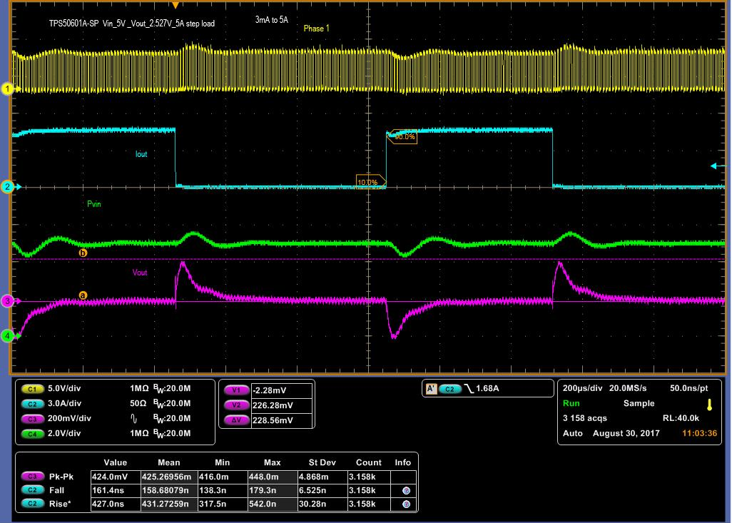
Application Curve

The evaluation module for the TPS50601A-SP was used to capture a load step response of the device. The testing conditions were:

  • VIN = PVIN = 5 V
  • VOUT = 2.5 V
  • Load step = 0 A to 5 A
  • Switching frequency = 100 kHz
TPS50601A-SP waveform01_slvub65.pngFigure 25. 5-A Step Response for 100-kHz Switching Operation