ZHCSNW0C February 2019 – April 2021 TPS51396A
PRODUCTION DATA
- 1 特性
- 2 应用
- 3 说明
- 4 Revision History
- 5 Pin Configuration and Functions
- 6 Specifications
- 7 Detailed Description
- 8 Application and Implementation
- 9 Power Supply Recommendations
- 10Layout
- 11Device and Documentation Support
- 12Mechanical, Packaging, and Orderable Information
封装选项
请参考 PDF 数据表获取器件具体的封装图。
机械数据 (封装 | 引脚)
- RJE|20
散热焊盘机械数据 (封装 | 引脚)
- RJE|20
订购信息
7.4.4 Mode Selection
The device reads the voltage on the MODE pin during start-up and latches onto one of the MODE options listed below in Table 7-1 . The voltage on the MODE pin can be set by connecting this pin to the center tap of a resistor divider connected between VCC and AGND. A guideline for the top resistor (RM_H) and the bottom resistor (RM_L) is shown in Table 7-1, and 1% resistors are recommended. It is important that the voltage for the MODE pin is derived from the VCC rail only since internally this voltage is referenced to detect the MODE option. The MODE pin setting can be reset only by a VIN power cycling or EN toggle.
| RM_H(kΩ) | RM_L (kΩ) | Light Load Operation | Switching Frequency (kHz) |
|---|---|---|---|
| 330 | 5.1 | Eco-mode | 600 |
| 330 | 15 | Eco-mode | 800 |
| 330 | 27 | Eco-mode | 1000 |
| 300 | 43 | OOA mode | 600 |
| 150 | 33 | OOA mode | 800 |
| 160 | 51 | OOA mode | 1000 |
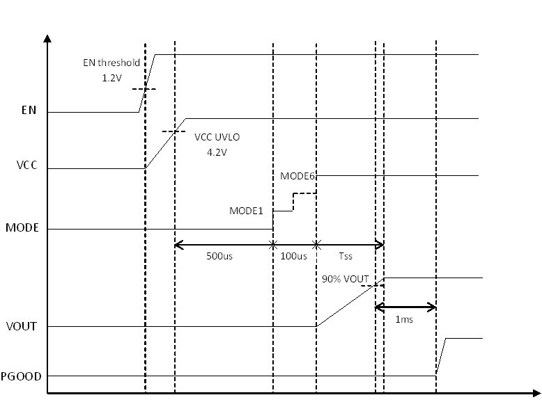
Figure 7-1 below shows the typical start-up sequence of the device once the enable signal crosses the EN turn on threshold. After the voltage on VCC crosses the rising UVLO threshold it takes about 500us to read the first mode setting and approximately 100us from there to finish the last mode setting. The output voltage starts ramping after the mode reading is done.
 Figure 7-1 Power-Up Sequence