ZHCSNW0C February 2019 – April 2021 TPS51396A
PRODUCTION DATA
- 1 特性
- 2 应用
- 3 说明
- 4 Revision History
- 5 Pin Configuration and Functions
- 6 Specifications
- 7 Detailed Description
- 8 Application and Implementation
- 9 Power Supply Recommendations
- 10Layout
- 11Device and Documentation Support
- 12Mechanical, Packaging, and Orderable Information
封装选项
请参考 PDF 数据表获取器件具体的封装图。
机械数据 (封装 | 引脚)
- RJE|20
散热焊盘机械数据 (封装 | 引脚)
- RJE|20
订购信息
5 Pin Configuration and Functions
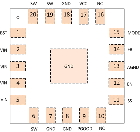
 Figure 5-1 RJE Package20-Pin VQFN
(Top View)
Figure 5-1 RJE Package20-Pin VQFN
(Top View)Table 5-1 Pin Functions
| PIN | I/O | DESCRIPTION | |
|---|---|---|---|
| NAME | NO. | ||
| BST | 1 | I | Supply input for the gate drive voltage of the high-side MOSFET. Connect the bootstrap capacitor between BST and SW, 0.1 μF is recommended. |
| VIN | 2,3,4,5 | P | Input voltage supply pin for the control circuitry. Connect the input decoupling capacitors between VIN and GND. |
| SW | 6,19,20 | O | Switch node terminal. Connect the output inductor to this pin. |
| GND | 7,8,18,Pad | G | Power GND terminal for the controller circuit and the internal circuitry. |
| PGOOD | 9 | O | Open drain power good indicator. It is asserted low if output voltage is out of PGOOD threshold, over voltage or if the device is under thermal shutdown, EN shutdown or during soft start. |
| SS | 11 | I | Soft-start time selection pin. Connecting an external capacitor sets the soft-start time and if no external capacitor is connected, the soft-start time is about 1.3 ms. |
| NC | 10,16 | Not connect. Can be connected to GND plane for better thermal achieved. | |
| EN | 12 | I | Enable pin of buck converter. EN pin is a digital input pin, decides turn on or off buck converter. Internal pull down current to disable converter if leave this pin open. |
| AGND | 13 | G | Ground of internal analog circuitry. Connect AGND to GND plane with a short trace. |
| FB | 14 | I | Converter feedback input. Connect to the center tap of the resistor divider between output voltage and AGND. |
| MODE | 15 | I | Llight load operation mode selection pin. Connect this pin to a resistor divider from VCC and AGND, the different MODE options are shown in Table 7-1 |
| VCC | 17 | O | 5.0-V internal VCC LDO output. This pin supplies voltage to the internal circuitry and gate driver. Bypass this pin with a 1-μF capacitor. |