ZHCSLU8A September 2020 – October 2020 TPS51397A
PRODUCTION DATA
- 1 特性
- 2 应用
- 3 说明
- 4 Revision History
- 5 Pin Configuration and Functions
- 6 Specifications
- 7 Detailed Description
- 8 Application and Implementation
- 9 Power Supply Recommendations
- 10Layout
- 11Device and Documentation Support
- 12Mechanical, Packaging, and Orderable Information
5 Pin Configuration and Functions
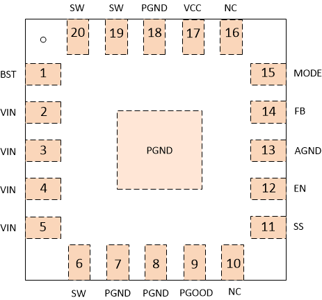
 Figure 5-1 20-Pin VQFN RJE Package (Top
View)
Figure 5-1 20-Pin VQFN RJE Package (Top
View)Table 5-1 Pin Functions
| PIN | I/O | DESCRIPTION | |
|---|---|---|---|
| NAME | NO. | ||
| BST | 1 |
O |
Supply input for the gate drive voltage of the high-side MOSFET. Connect the bootstrap capacitor between BST and SW. 0.1 μF is recommended. |
| VIN | 2,3,4,5 | P | Input voltage supply pin for the control circuitry. Connect the input decoupling capacitors between VIN and PGND. |
| SW | 6,19,20 | O | Switching node connection to the inductor and bootstrap capacitor for buck. This pin voltage swings from a diode voltage below the ground up to input voltage of buck. |
| PGND | 7,8,18, Thermal Pad | G | Power GND terminal for the controller circuit and the internal circuitry |
| PGOOD | 9 | O | Open-drain power-good indicator. It is asserted low if output voltage is out of PG threshold, over voltage, or if the device is under thermal shutdown, EN shutdown, or during soft start. |
| SS | 11 |
O |
Soft-Start time selection pin. Connecting an external capacitor sets the soft-start time and if no external capacitor is connected, the soft-start time is about 1.2 ms. |
| NC | 10,16 | Not connect. Can be connected to GND plane for better thermal achieved. | |
| EN | 12 | I | Enable input of buck converter |
| AGND | 13 | G | Ground of internal analog circuitry. Connect AGND to GND plane with a short trace. |
| FB | 14 | I | Feedback sensing pin for Buck output voltage. Connect this pin to the resistor divider between output voltage and AGND. |
| MODE | 15 | I | Switching frequency and light load operation mode selection pin. Connect this pin to a resistor divider from VCC and AGND for different MODE options shown in Table 7-1. |
| VCC | 17 | O | The driver and control circuits are powered from this voltage. Decouple with a minimum 1-μF ceramic capacitor as close to VCC as possible. |