ZHCS936A May 2012 – February 2019 TPS53014
PRODUCTION DATA.
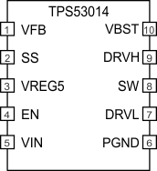
5 Pin Configuration and Functions
DGS Package
10-Pin VSSOP
Top View

Pin Functions
| PIN | I/O | DESCRIPTION | |
|---|---|---|---|
| NAME | VSSOP-10 | ||
| VFB | 1 | I | D-CAP2 feedback input. Connect to output voltage with resistor divider. |
| SS | 2 | O | Soft start programming pin. Connect capacitor from SS pin to GND to program soft start time. |
| VREG5 | 3 | O | Output of 5-V linear regulator and supply for MOSFET driver. Bypass to GND with a minimum 4.7-μF high quality ceramic capacitor. VREG5 is active when EN is asserted high. |
| EN | 4 | I | Enable. Pull High to enable converter. |
| VIN | 5 | I | Supply Input for 5-V linear regulator. Bypass to GND with a minimum 0.1-μF high quality ceramic capacitor. |
| PGND | 6 | I | System ground. |
| DRVL | 7 | O | Low-side N-Channel MOSFET gate driver output. PGND referenced driver switches between PGND(OFF) and VREG5(ON). |
| SW | 8 | I/O | Switch node connections for both the high-side driver and over current comparator. |
| DRVH | 9 | O | High-side N-channel MOSFET gate driver output. SW referenced driver switches between SW(OFF) and VBST(ON). |
| VBST | 10 | I | High-side MOSFET gate driver bootstrap voltage input. Connect a capacitor from VBST to SW. An internal diode is connected between VREG5 and VBST |