ZHCSTR3B December 2010 – November 2023 TPS53315
PRODUCTION DATA
- 1
- 1 特性
- 2 应用
- 3 说明
- 4 Pin Configuration and Functions
- 5 Specifications
-
6 Detailed Description
- 6.1 Overview
- 6.2 Functional Block Diagram
- 6.3
Feature Description
- 6.3.1 D-CAP™ Integrated Circuit with Adaptive On-Time
- 6.3.2 Small Signal Model
- 6.3.3 Ramp Signal
- 6.3.4 Auto-Skip Eco-mode Light Load Operation
- 6.3.5 Adaptive Zero Crossing
- 6.3.6 Forced Continuous Conduction Mode
- 6.3.7 Power Good
- 6.3.8 Current Sense and Overcurrent Protection
- 6.3.9 Overvoltage and Undervoltage Protection
- 6.3.10 UVLO Protection
- 6.3.11 Thermal Shutdown
- 6.4 Device Functional Modes
-
7 Application and Implementation
- 7.1 Application Information
- 7.2
Typical Application
- 7.2.1
Typical Application Circuit Diagram
- 7.2.1.1 Design Requirements
- 7.2.1.2
Detailed Design Procedure
- 7.2.1.2.1 Step 1: Select Operation Mode and Soft-Start Time
- 7.2.1.2.2 Step 2: Select Switching Frequency
- 7.2.1.2.3 Step 3: Select the Inductance
- 7.2.1.2.4 Step 4: Select Output Capacitors
- 7.2.1.2.5 Step 5: Determine the Voltage-Divider Resistance (R1 and R2)
- 7.2.1.2.6 Step 6: Select the Overcurrent Resistance (RTRIP)
- 7.2.1.3 Application Curves
- 7.2.2 Typical Application Circuit Diagram With Ceramic Output Capacitors
- 7.2.1
Typical Application Circuit Diagram
- 7.3 Power Supply Recommendations
- 7.4 Layout
- 8 Device and Documentation Support
- 9 Revision History
- 10Mechanical, Packaging, and Orderable Information
5.6 Typical Characteristics
Inductor Values: IN06155: 1 µH, 2.3 mΩ, HCB1175-501: 0.5 µH, 0.29 mΩ
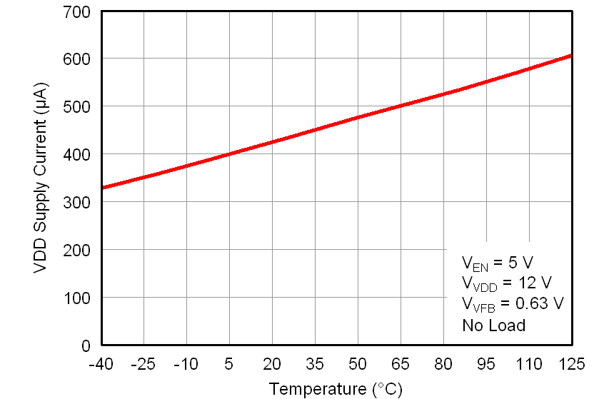 Figure 5-1 VDD Supply Current vs Temperature
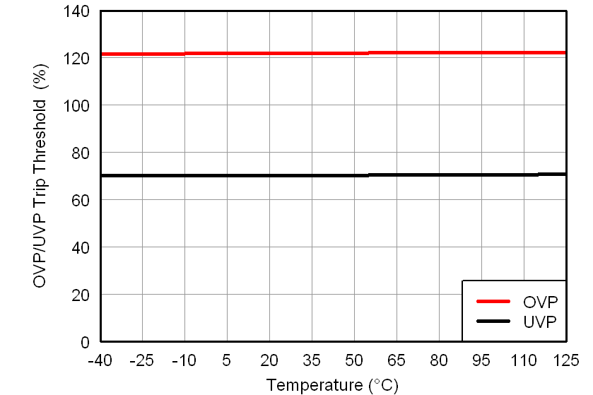 Figure 5-3 OVP/UVP Trip Threshold vs Temperature
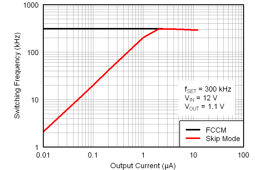 Figure 5-5 Frequency vs Temperature (fSET = 300 kHz)
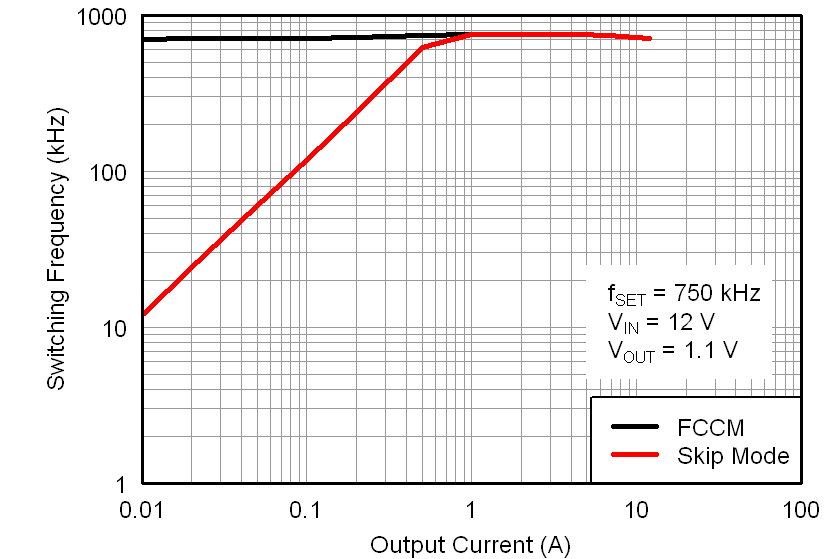 Figure 5-7 Frequency vs Temperature (fSET = 750 kHz)
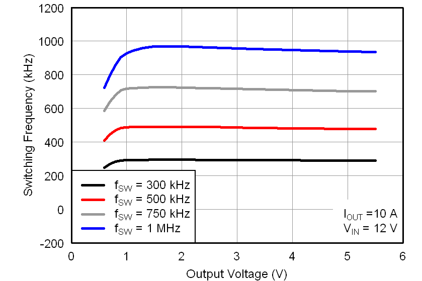 Figure 5-9 Switching Frequency vs Output Voltage
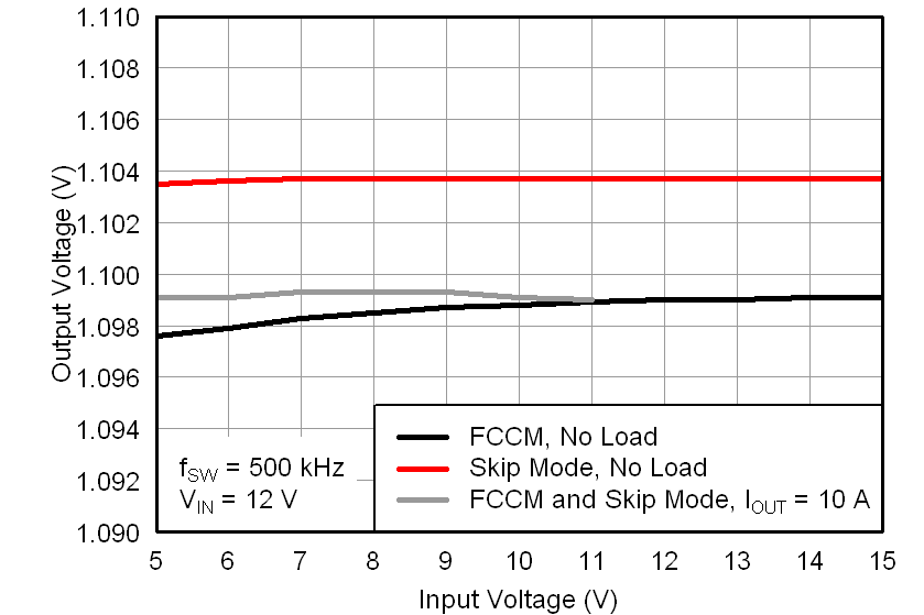 Figure 5-11 Output Voltage vs Input Voltage
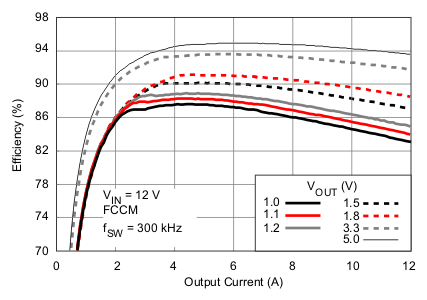
| Inductors: VOUT ≤ 1.8 V: HCB1175-501, VOUT ≥ 3.3 V: IN06155 |
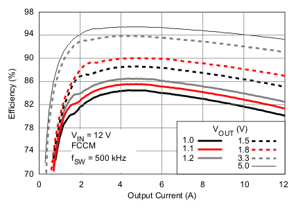
| Inductors: VOUT ≤ 1.8 V: HCB1175-501, VOUT ≥ 3.3 V: IN06155 |
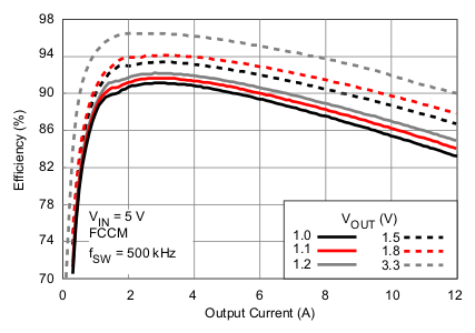
| Inductor: HCB1175-501 |
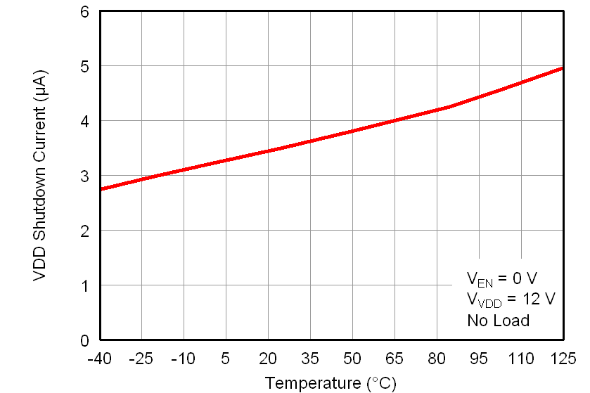 Figure 5-2 VDD Shutdown Current vs Temperature
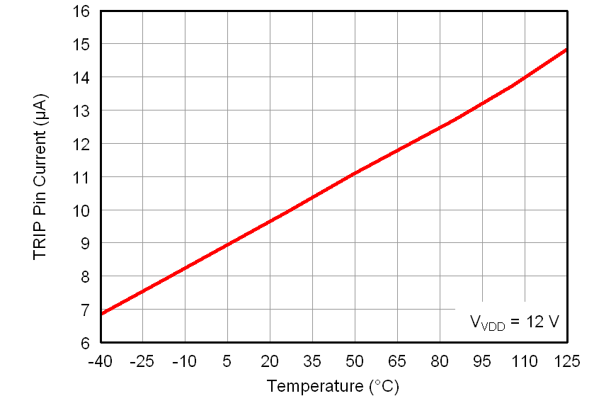 Figure 5-4 Trip Pin Current vs Temperature
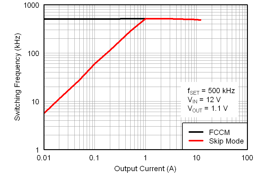 Figure 5-6 Frequency vs Temperature (fSET = 500 kHz)
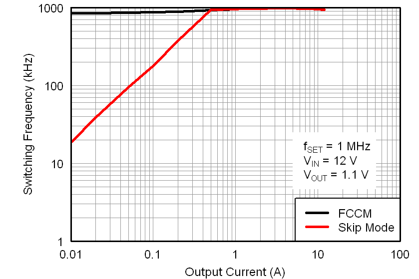 Figure 5-8 Frequency vs Temperature (fSET = 1 MHz)
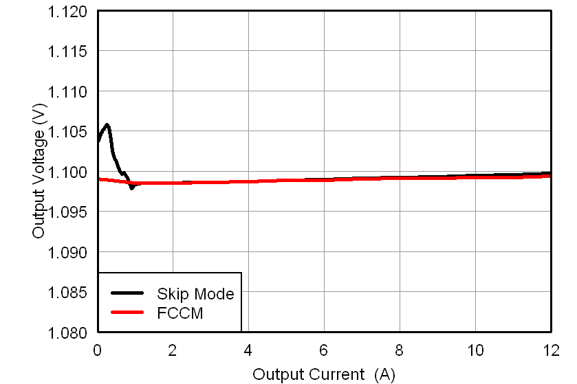 Figure 5-10 Output Voltage vs Output Current
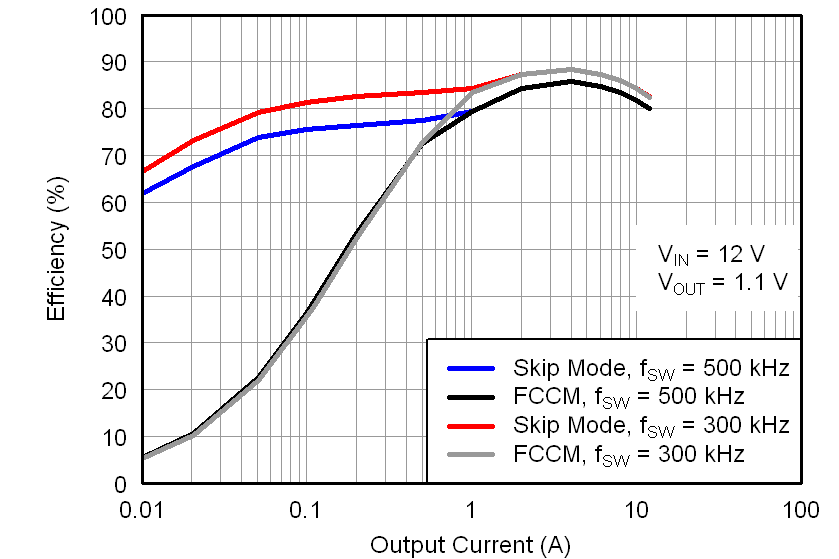 Figure 5-12 Efficiency vs Output Current, Inductor: IN06155
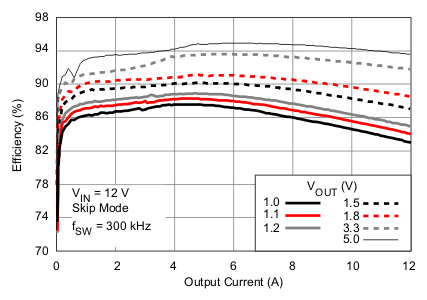
| Inductors: VOUT ≤ 1.8 V: HCB1175-501, VOUT ≥ 3.3 V: IN06155 |
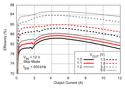
| Inductors: VOUT ≤ 1.8 V: HCB1175-501, VOUT ≥ 3.3 V: IN06155 |
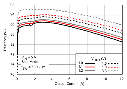
| Inductor: HCB1175-501 |