ZHCSED1A November 2015 – November 2015 TPS53317A
PRODUCTION DATA.
- 1 特性
- 2 应用
- 3 说明
- 4 修订历史记录
- 5 Pin Configuration and Functions
- 6 Specifications
- 7 Detailed Description
- 8 Application and Implementation
- 9 Power Supply Recommendations
- 10Layout
- 11器件和文档支持
- 12机械、封装和可订购信息
7 Detailed Description
7.1 Overview
The TPS53317A device is a D-CAP+™ mode adaptive on-time converter. Integrated high-side and low-side FETs support a maximum of 6-A DC output current. The converter automatically operates in discontinuous conduction mode (DCM) to optimize light-load efficiency. Multiple switching frequencies are provided to enable optimization of the power train for the cost, size and efficiency requirements of the design (see Table 1).
In adaptive on-time converters, the controller varies the on-time as a function of input and output voltage to maintain a nearly constant frequency during steady-state conditions. In conventional constant on-time converters, each cycle begins when the output voltage crosses to a fixed reference level. However, in the TPS53317A device, the cycle begins when the current feedback reaches an error voltage level which is the amplified difference between the reference voltage and the feedback voltage.
7.2 Functional Block Diagram
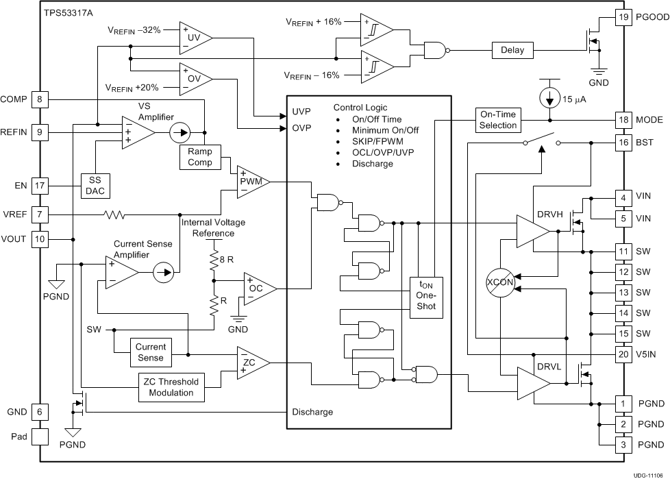
7.3 Feature Description
7.3.1 PWM Operation
Referring to Figure 17, in steady state, continuous conduction mode, the converter operates in the following way.
Starting with the condition that the top FET is off and the bottom FET is on, the current feedback (VCS) is higher than the error amplifier output (VCOMP). VCS falls until it hits VCOMP, which contains a component of the output ripple voltage. VCS is not directly accessible by measuring signals on pins of TPS53317A device. The PWM comparator senses where the two waveforms cross and triggers the on-time generator.
 Figure 17. D-CAP+™ Mode Basic Waveforms
The current feedback is an amplified and filtered version of the voltage between PGND and SW during low-side FET on-time. The device also provides a single-ended voltage (VOUT) feedback to increase the system accuracy and reduce the dependence of circuit performance on layout.
7.3.2 PWM Frequency and Adaptive On-Time Control
In general, the on-time (at the SW node) can be estimated by Equation 1.

where
- fSW is the frequency selected by the connection of the MODE pin
The on-time pulse is sent to the top FET. The inductor current and the current feedback rises to peak value. Each ON pulse is latched to prevent double pulsing. Switching frequency settings are shown in Table 1.
7.3.3 Light-Load Power Saving Features
The TPS53317A device has an automatic pulse-skipping mode to provide excellent efficiency over a wide load range. The converter senses inductor current and prevents negative flow by shutting off the low-side gate driver. This saves power by eliminating re-circulation of the inductor current. Further, when the bottom FET shuts off, the converter enters discontinuous mode, and the switching frequency decreases, thus reducing switching losses as well.
The device also provides a special light-load power saving feature, called ripple reduction. Essentially, it reduces the on-time in SKIP mode to effectively reduce the output voltage ripple associated with using an all MLCC capacitor output power stage design.
7.3.4 Power Sequences
7.3.4.1 Non-Tracking Startup
The TPS53317A device can be configured for non-tracking application. When non-tracking is configured, output voltage is regulated to the REFIN voltage which taps off the voltage dividers from the 2-V reference voltage. Either the EN pin or the V5IN pin can be used to start up the device. The device uses internal voltage servo DAC to provide a 1.6-ms soft-start time during soft-start initialization. (See Figure 19.)
In a non-tracking application, the output voltage is determined by the resistive divider between the VREF pin and the REFIN pin.

.
.
 Figure 18. Non-Tracking Configuration
 Figure 19. Non-Tracking Startup Timing
7.3.4.2 Tracking Startup
The TPS53317A device can also be configured for tracking application. When tracking configuration is desired, output voltage is also regulated to the REFIN voltage which comes from an external power source. In order for the device to differentiate between a non-tracking configuration or a tracking configuration, there is a minimum delay time of 260 µs required between the time when VREF reaches 2 V to the time when the REFIN pin voltage can be applied, in order for the device to track properly (see Figure 22). The valid REFIN voltage range is between 0.45 V and 2 V.
In a tracking application, the output voltage should be one half of the VDDQ voltage. VDDQ can be VIN or it can be an additional voltage rail. Thus, R1= R2 both in Figure 20 and Figure 21.

 Figure 20. Tracking Configuration 1
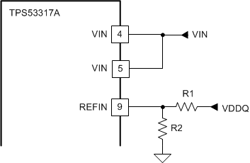 Figure 21. Tracking Configuration 2
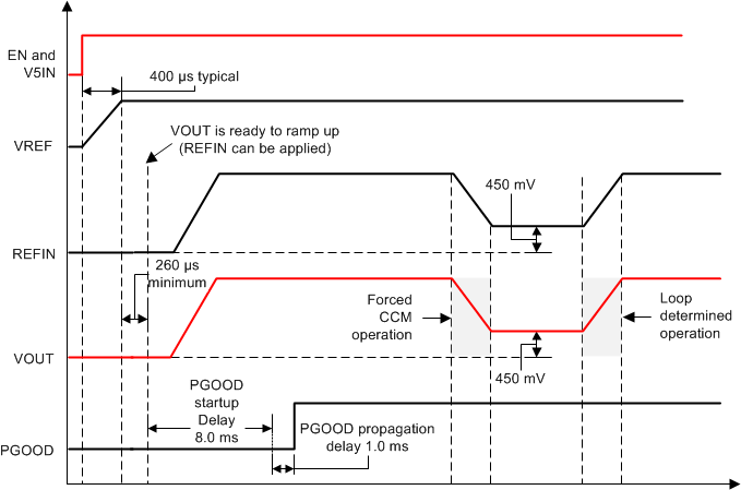 Figure 22. Tracking Startup Timing
Select PWM mode for an application that requires external tracking, because the output voltage can not be decreased during a no-load condition when the device operates in SKIP mode.
7.3.5 Protection Features
The TPS53317A device offers many features to protect the converter power train as well as the system electronics.
7.3.5.1 5-V Undervoltage Protection (UVLO)
The TPS53317A device continuously monitors the voltage on the V5IN pin to ensure that the voltage level is high enough to bias the device properly and to provide sufficient gate drive potential to maintain high efficiency. The converter starts with approximately 4.3 V and has a nominal 440 mV of hysteresis. If the 5-V UVLO limit is reached, the converter transitions the phase node into an off function, and the converter remains in the off state until the device is reset by cycling the 5-V supply until the 5-V POR is reached (2.3-V nominal). The power input does not have a UVLO function.
7.3.5.2 Power Good Signals
The TPS53317A device has one open-drain power good (PGOOD) pin. During startup, there is a 1-ms power good high propagation delay. The PGOOD pin de-asserts as soon as the EN pin is pulled low or an undervoltage condition on V5IN or any other fault is detected.
7.3.5.3 Output Overvoltage Protection (OVP)
In addition to the power good function described above, the TPS53317A device has additional OVP and UVP thresholds and protection circuits.
An OVP condition is detected when the output voltage is approximately 120% × VREFIN. In this case, the converter de-asserts the PGOOD signals and performs the overvoltage protection function. During OVP, the low-side FET is always on before triggering a negative overcurrent. When a negative OC is also tripped, the low-side FET is no longer continuously on, and pulsed signals are generated to limit the negative inductor current. When the VOUT pin voltage drops below 250 mV, the low-side FET turns off and the converter latches off. The converter remains in the off state until the device is reset by cycling the 5-V supply until the 5-V POR is reached (2.3-V nominal) or when the EN pin is toggled off and on.
7.3.5.4 Output Undervoltage Protection (UVP)
Output undervoltage protection works in conjunction with the current protection described in the Overcurrent Protection and Overcurrent Limit sections. If the output voltage drops below 68% of VREFIN, after approximately a 250-µs delay, the device stops switching and enters hiccup mode. After a hiccup waiting time, a restart is attempted. If the fault condition is not cleared, hiccup mode operation may continue indefinitely.
7.3.5.5 Overcurrent Protection
Both positive and negative overcurrent protection are provided in the TPS53317A device.
- Overcurrent Limit (OCL)
- Negative OCL
7.3.5.5.1 Overcurrent Limit
If the sensed current value is above the OCL setting, the converter delays the next ON pulse until the current drops below the OCL limit. Current limiting occurs on a pulse-by-pulse basis. The device uses a valley current limiting scheme where the DC OCL trip point is the OCL limit plus half of the inductor ripple current. The typical valley OCL threshold is 7.6 A or 5.4 A (depending on mode selection). The average output current limit calculation is shown in Equation 4.
During the overcurrent protection event, the output voltage droops if the duty cycle cannot satisfy output voltage requirements and continues to droop until the UVP limit is reached. Then, the converter de-asserts the PGOOD pin, and then enters hiccup mode after a 250-µs delay. The converter remains in hiccup mode until the fault is cleared.

7.3.5.5.2 Negative OCL
The negative OCL circuit acts when the converter is sinking current from the output capacitor(s). The converter continues to act in a valley mode, the typical value of the negative OCL set point is –9.3 A or –6.5 A (depending on mode selection).
7.3.6 Thermal Protection
The TPS53317A device has an internal temperature sensor. When the temperature reaches a nominal 145°C, the device shuts down until the temperature decreases by approximately 10°C, when the converter restarts.
7.4 Device Functional Modes
7.4.1 Non-Droop Configuration
The TPS53317A device can be configured as a non-droop solution. The benefit of a non-droop approach is that load regulation is flat, therefore, in a system where tight DC tolerance is desired, the non-droop approach is recommended. For the Intel system agent application, non-droop is recommended as the standard configuration.
The non-droop approach can be implemented by connecting a resistor and a capacitor between the COMP and the VREF pins. The purpose of the type II compensation is to obtain high DC feedback gain while minimizing the phase delay at unity gain cross over frequency of the converter.
The value of the resistor (RC) can be calculated using the desired unity gain bandwidth of the converter, and the value of the capacitor (CC) can be calculated by knowing where the zero location is desired. The capacitor CP is optional, but recommended. Its appropriate capacitance value can be calculated using the desired pole location.
Figure 23 shows the basic implementation of the non-droop mode using the device
 Figure 23. Non-Droop Mode Basic Implementation
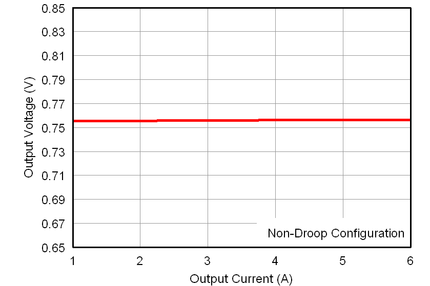
Figure 24 shows shows the load regulation using non-droop configuration.
Figure 25 shows the transient response of the device using non-droop configuration, where COUT = 3 x 47 µF. The applied step load is from 0 A to 2 A.
| VIN = 1.5 V | VOUT = 0.75 V | |
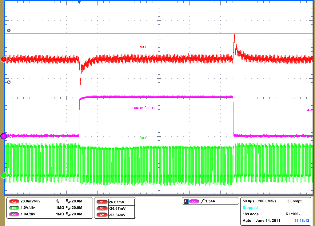
| CH 2: VOUT
(20 mV/div) |
CH 4: IOUT
(1 A/div) |
CH 3: SW (1 V/div) |
7.4.2 Droop Configuration
The terminology for droop is the same as load line or voltage positioning as defined in the Intel CPU VCORE specification. Based on the actual tolerance requirement of the application, load-line set points can be defined to maximize either cost savings (by reducing output capacitors) or power reduction benefits.
Accurate droop voltage response is provided by the finite gain of the droop amplifier. The equation for droop voltage is shown in Equation 5.

where
- low-side on-resistance is used as the current sensing element
- ACSINT is a constant, which nominally is 53 mV/A.
- IOUT is the DC current of the inductor, or the load current
- RDROOP is the value of resistor from the COMP pin to the VREF pin
- gM is the transconductance of the droop amplifier with nominal value of 1 mS
Equation 6 can be used to easily derive RDROOP for any load line slope/droop design target.

Choose a value for the RDROOP resistor that is below 20 kΩ. More than 20 kΩ of droop resistance may cause the loop to become unstable.
Figure 26 shows the basic implementation of the droop mode using the TPS53317A device.
 Figure 26. DROOP Mode Basic Implementation
The droop (voltage positioning) method was originally recommended to reduce the number of external output capacitors required. The effective transient voltage range is increased because of the active voltage positioning (see Figure 27).
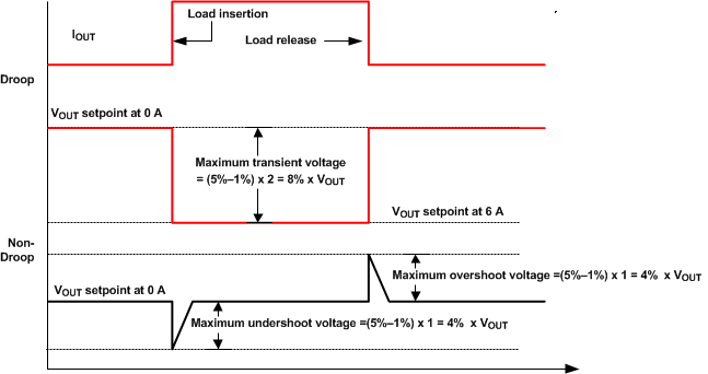 Figure 27. DROOP vs Non-DROOP in Transient Voltage Window
In applications where the DC and the AC tolerances are not separated, (meaning that there is no strict DC tolerance requirement) the droop method can be used.
Table 1. Mode Definitions
| MODE | MODE RESISTANCE (kΩ) | LIGHT-LOAD POWER SAVING MODE | SWITCHING FREQUENCY (fSW) |
OVERCURRENT LIMIT (OCL) VALLEY (A) |
|---|---|---|---|---|
| 1 | 0 | SKIP | 600 kHz | 7.6 |
| 2 | 12 | 600 kHz | 5.4 | |
| 3 | 22 | 1 MHz | 5.4 | |
| 4 | 33 | 1 MHz | 7.6 | |
| 5 | 47 | PWM | 600 kHz | 7.6 |
| 6 | 68 | 600 kHz | 5.4 | |
| 7 | 100 | 1 MHz | 5.4 | |
| 8 | OPEN | 1 MHz | 7.6 |
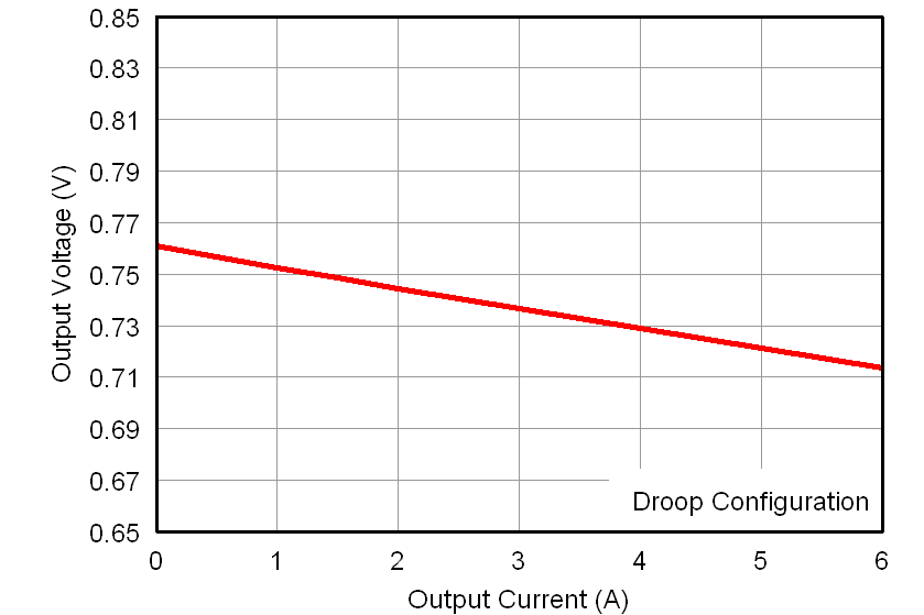
Figure 28 shows the load regulation of the 1.5-V rail using an RDROOP value of 6.8 kΩ.
Figure 29 shows the transient response of the TPS53317A device using droop configuration and COUT = 3 × 47 µF. The applied step load is from 0 A to 2 A.
| VIN = 1.5 V | VOUT = 0.75 V | |

| CH 2: VOUT
(20 mV/div) |
CH 4: IOUT
(1 A/div) |
CH 3: SW (1 V/div) |