ZHCS979F June 2012 – October 2020 TPS53318 , TPS53319
PRODUCTION DATA
- 1 特性
- 2 应用
- 3 说明
- 4 Revision History
- 5 Device Comparison Table
- 6 Pin Configuration and Functions
- 7 Specifications
-
8 Detailed Description
- 8.1 Overview
- 8.2 Functional Block Diagram
- 8.3
Feature Description
- 8.3.1 5-V LDO and VREG Start-Up
- 8.3.2 Adaptive On-Time D-CAP Control and Frequency Selection
- 8.3.3 Ramp Signal
- 8.3.4 Adaptive Zero Crossing
- 8.3.5 Output Discharge Control
- 8.3.6 Power-Good
- 8.3.7 Current Sense, Overcurrent, and Short Circuit Protection
- 8.3.8 Overvoltage and Undervoltage Protection
- 8.3.9 Redundant Overvoltage Protection (OVP)
- 8.3.10 UVLO Protection
- 8.3.11 Thermal Shutdown
- 8.3.12 Small Signal Model
- 8.3.13 External Component Selection Using All Ceramic Output Capacitors
- 8.4 Device Functional Modes
-
9 Application and Implementation
- 9.1 Application Information
- 9.2
Typical Applications
- 9.2.1
Application Using Bulk Output Capacitors, Redundant Overvoltage Protection Function (OVP) Disabled
- 9.2.1.1 Design Requirements
- 9.2.1.2
Detailed Design Procedure
- 9.2.1.2.1 Step One: Select Operation Mode and Soft-Start Time
- 9.2.1.2.2 Step Two: Select Switching Frequency
- 9.2.1.2.3 Step Three: Choose the Inductor
- 9.2.1.2.4 Step Four: Choose the Output Capacitor or Capacitors
- 9.2.1.2.5 Step Five: Determine the Value of R1 and R2
- 9.2.1.2.6 Step Six: Choose the Overcurrent Setting Resistor
- 9.2.1.3 Application Curves
- 9.2.2 Application Using Ceramic Output Capacitors, Redundant Overvoltage Protection Function (OVP) Enabled
- 9.2.1
Application Using Bulk Output Capacitors, Redundant Overvoltage Protection Function (OVP) Disabled
- 10Power Supply Recommendations
- 11Layout
- 12Device and Documentation Support
- 13Mechanical, Packaging, and Orderable Information
7.6 Typical Characteristics
 Figure 7-1 VDD Supply Current vs. Junction Temperature
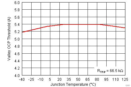 Figure 7-3 Valley OCP Threshold vs Temperature
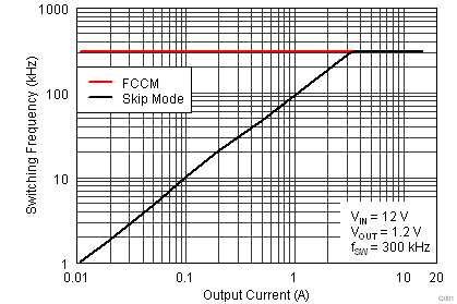 Figure 7-5 Switching Frequency vs. Output Current
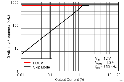 Figure 7-7 Switching Frequency vs. Output Current
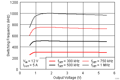 Figure 7-9 Switching Frequency vs. Output Voltage
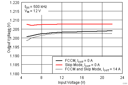 Figure 7-11 Output Voltage vs. Input Voltage
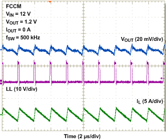 Figure 7-13 1.2-V Output FCCM Mode Steady-State Operation
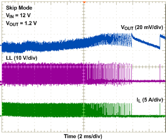 Figure 7-15 CCM to DCM Transition
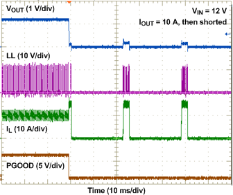 Figure 7-17 Short Circuit Protection
 Figure 7-2 VDD Shutdown Current vs. Junction Temperature
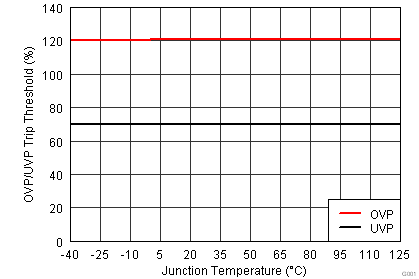 Figure 7-4 OVP/UVP Trip Threshold vs. Junction Temperature
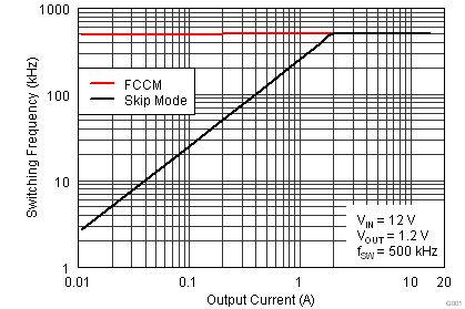 Figure 7-6 Switching Frequency vs. Output Current
 Figure 7-8 Switching Frequency vs. Output Current
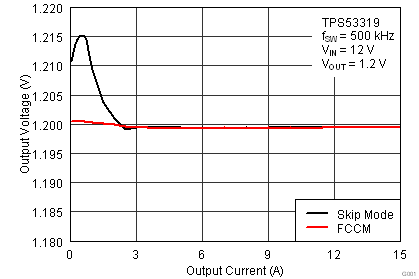 Figure 7-10 Output Voltage vs. Output Current
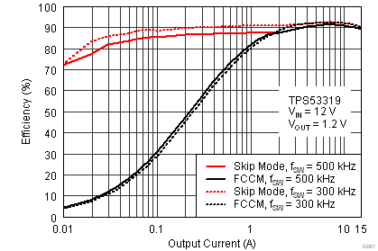 Figure 7-12 Efficiency vs Output Current
 Figure 7-14 1.2-V Output Skip Mode Steady-State Operation
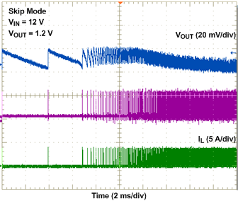 Figure 7-16 DCM to CCM Transition