ZHCS979F June 2012 – October 2020 TPS53318 , TPS53319
PRODUCTION DATA
- 1 特性
- 2 应用
- 3 说明
- 4 Revision History
- 5 Device Comparison Table
- 6 Pin Configuration and Functions
- 7 Specifications
-
8 Detailed Description
- 8.1 Overview
- 8.2 Functional Block Diagram
- 8.3
Feature Description
- 8.3.1 5-V LDO and VREG Start-Up
- 8.3.2 Adaptive On-Time D-CAP Control and Frequency Selection
- 8.3.3 Ramp Signal
- 8.3.4 Adaptive Zero Crossing
- 8.3.5 Output Discharge Control
- 8.3.6 Power-Good
- 8.3.7 Current Sense, Overcurrent, and Short Circuit Protection
- 8.3.8 Overvoltage and Undervoltage Protection
- 8.3.9 Redundant Overvoltage Protection (OVP)
- 8.3.10 UVLO Protection
- 8.3.11 Thermal Shutdown
- 8.3.12 Small Signal Model
- 8.3.13 External Component Selection Using All Ceramic Output Capacitors
- 8.4 Device Functional Modes
-
9 Application and Implementation
- 9.1 Application Information
- 9.2
Typical Applications
- 9.2.1
Application Using Bulk Output Capacitors, Redundant Overvoltage Protection Function (OVP) Disabled
- 9.2.1.1 Design Requirements
- 9.2.1.2
Detailed Design Procedure
- 9.2.1.2.1 Step One: Select Operation Mode and Soft-Start Time
- 9.2.1.2.2 Step Two: Select Switching Frequency
- 9.2.1.2.3 Step Three: Choose the Inductor
- 9.2.1.2.4 Step Four: Choose the Output Capacitor or Capacitors
- 9.2.1.2.5 Step Five: Determine the Value of R1 and R2
- 9.2.1.2.6 Step Six: Choose the Overcurrent Setting Resistor
- 9.2.1.3 Application Curves
- 9.2.2 Application Using Ceramic Output Capacitors, Redundant Overvoltage Protection Function (OVP) Enabled
- 9.2.1
Application Using Bulk Output Capacitors, Redundant Overvoltage Protection Function (OVP) Disabled
- 10Power Supply Recommendations
- 11Layout
- 12Device and Documentation Support
- 13Mechanical, Packaging, and Orderable Information
8.3.2 Adaptive On-Time D-CAP Control and Frequency Selection
Neither the TPS53318 nor the TPS53319 device have a dedicated oscillator to determine switching frequency. However, the device operates with pseudo-constant frequency by feedforwarding the input and output voltages into the on-time one-shot timer. The adaptive on-time control adjusts the on-time to be inversely proportional to the input voltage and proportional to the output voltage as shown in Equation 1.

This makes the switching frequency fairly constant in steady state conditions over a wide input voltage range. The switching frequency is selectable from eight preset values by a resistor connected between the RF pin and GND or between the RF pin and the VREG pin as shown in Table 8-1. Maintaining open resistance sets the switching frequency to 500 kHz.
| RESISTOR (RRF) CONNECTIONS | SWITCHING FREQUENCY (fSW) (kHz) | |
|---|---|---|
| VALUE (kΩ) | CONNECT TO | |
| 0 | GND | 250 |
| 187 | GND | 300 |
| 619 | GND | 400 |
| OPEN | n/a | 500 |
| 866 | VREG | 600 |
| 309 | VREG | 750 |
| 124 | VREG | 850 |
| 0 | VREG | 970 |
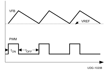
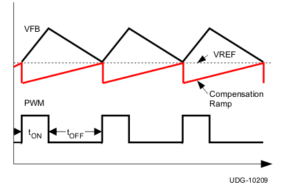
The off-time is modulated by a PWM comparator. The VFB node voltage (the mid-point of resistor divider) is compared to the internal 0.6-V reference voltage added with a ramp signal. When both signals match, the PWM comparator asserts a set signal to terminate the off-time (turn off the low-side MOSFET and turn on high-side the MOSFET). The set signal is valid if the inductor current level is below the OCP threshold, otherwise the off-time is extended until the current level falls below the threshold.
The waveforms shown in Figure 8-2 show on-time control without ramp compensation. The waveforms shown in Figure 8-3 show on-time control without ramp compensation.
 Figure 8-2 On-Time Control Without Ramp Compensation
 Figure 8-3 On-Time Control With Ramp Compensation