ZHCS181G August 2011 – April 2021 TPS53355
PRODUCTION DATA
- 1 特性
- 2 应用
- 3 说明
- 4 Revision History
- 5 Pin Configuration and Functions
- 6 Specifications
-
7 Detailed Description
- 7.1 Overview
- 7.2 Functional Block Diagram
- 7.3
Feature Description
- 7.3.1 5-V LDO and VREG Start-Up
- 7.3.2 Adaptive On-Time D-CAP Control and Frequency Selection
- 7.3.3 Ramp Signal
- 7.3.4 Adaptive Zero Crossing
- 7.3.5 Power-Good
- 7.3.6 Current Sense, Overcurrent and Short Circuit Protection
- 7.3.7 Overvoltage and Undervoltage Protection
- 7.3.8 UVLO Protection
- 7.3.9 Thermal Shutdown
- 7.4 Device Functional Modes
- 8 Application and Implementation
- 9 Power Supply Recommendations
- 10Layout
- 11Device and Documentation Support
- 12Mechanical, Packaging, and Orderable Information
封装选项
请参考 PDF 数据表获取器件具体的封装图。
机械数据 (封装 | 引脚)
- DQP|22
散热焊盘机械数据 (封装 | 引脚)
- DQP|22
订购信息
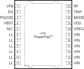
5 Pin Configuration and Functions

N/C = no connection
Figure 5-1 Package With PowerPad22-Pins
(LSON-CLIP)Top ViewTable 5-1 Pin Functions
| PIN | I/O/P(1) | DESCRIPTION | ||
|---|---|---|---|---|
| NAME | NO | |||
| EN | 2 | I | Enable pin. Typical turn-on threshold voltage is 1.2 V. Typical turn-off threshold is 0.95 V. | |
| GND | — | — | Ground and thermal pad of the device. Use proper number of vias to connect to ground plane. | |
| LL | 6 | B | Output of converted power. Connect this pin to the output Inductor. | |
| 7 | ||||
| 8 | ||||
| 9 | ||||
| 10 | ||||
| 11 | ||||
| MODE | 20 | I | Soft-start and Skip/CCM selection. Connect a resistor to select soft-start time using Table 7-3. The soft-start time is detected and stored into internal register during start-up. | |
| N/C | 5 | No connect. | ||
| PGOOD | 3 | O | Open drain power good flag. Provides 1-ms start-up delay after VFB falls in specified limits. When VFB goes out of the specified limits PGOOD goes low after a 2-µs delay. | |
| RF | 22 | I | Switching frequency selection. Connect a resistor to GND or VREG to select switching frequency using Table 7-1. The switching frequency is detected and stored during the startup. | |
| TRIP | 21 | I | OCL detection threshold setting pin. ITRIP = 10 µA at room temperature, 4700 ppm/°C current is sourced and set the OCL trip voltage as follows: | |
| VOCL = VTRIP/32 | (VTRIP ≤ 2.4 V, VOCL ≤ 75 mV) | |||
| VBST | 4 | P | Supply input for high-side FET gate driver (boost terminal). Connect capacitor from this pin to LL node. Internally connected to VREG via bootstrap MOSFET switch. | |
| VDD | 19 | P | Controller power supply input. VDD input voltage range is from 4.5 V to 25 V. | |
| VFB | 1 | I | Output feedback input. Connect this pin to Vout through a resistor divider. | |
| VIN | 12 | P | Conversion power input. VIN input voltage range is from 1.5 V to 15 V. | |
| 13 | ||||
| 14 | ||||
| 15 | ||||
| 16 | ||||
| 17 | ||||
| VREG | 18 | P | 5-V low drop out (LDO) output. Supplies the internal analog circuitry and driver circuitry. | |
(1) I=Input, O=Output, B=Bidirectional, P=Supply