ZHCSBM9C SEPTEMBER   2013  – June 2018 TPS53513

PRODUCTION DATA.  

  1. 特性
  2. 应用
  3. 说明
    1.     Device Images
      1.      简化原理图
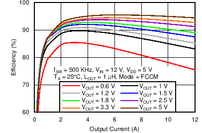
      2.      效率
  4. 修订历史记录
  5. Pin Configuration and Functions
    1.     Pin Functions
  6. Specifications
    1. 6.1 Absolute Maximum Ratings
    2. 6.2 ESD Ratings
    3. 6.3 Recommended Operating Conditions
    4. 6.4 Thermal Information
    5. 6.5 Electrical Characteristics
    6. 6.6 Typical Characteristics
  7. Detailed Description
    1. 7.1 Overview
    2. 7.2 Functional Block Diagram
    3. 7.3 Feature Description
      1. 7.3.1  5-V LDO and VREG Start-Up
      2. 7.3.2  Enable, Soft Start, and Mode Selection
      3. 7.3.3  Frequency Selection
      4. 7.3.4  D-CAP3 Control and Mode Selection
        1. 7.3.4.1 D-CAP3 Mode
        2. 7.3.4.2 Sample and Hold Circuitry
        3. 7.3.4.3 Adaptive Zero-Crossing
      5. 7.3.5  Power-Good
      6. 7.3.6  Current Sense and Overcurrent Protection
      7. 7.3.7  Overvoltage and Undervoltage Protection
      8. 7.3.8  Out-Of-Bounds Operation
      9. 7.3.9  UVLO Protection
      10. 7.3.10 Thermal Shutdown
    4. 7.4 Device Functional Modes
      1. 7.4.1 Auto-Skip Eco-mode Light Load Operation
      2. 7.4.2 Forced Continuous-Conduction Mode
  8. Application and Implementation
    1. 8.1 Application Information
    2. 8.2 Typical Application
      1. 8.2.1 Design Requirements
      2. 8.2.2 Detailed Design Procedure
        1. 8.2.2.1 Choose the Switching Frequency
        2. 8.2.2.2 Choose the Operation Mode
        3. 8.2.2.3 Choose the Inductor
        4. 8.2.2.4 Choose the Output Capacitor
        5. 8.2.2.5 Determine the Value of R1 and R2
      3. 8.2.3 Application Curves
  9. Power Supply Recommendations
  10. 10Layout
    1. 10.1 Layout Guidelines
    2. 10.2 Layout Example
    3. 10.3 Thermal Performance
  11. 11器件和文档支持
    1. 11.1 文档支持
      1. 11.1.1 使用 WEBENCH® 工具创建定制设计方案
    2. 11.2 文档支持
      1. 11.2.1 相关文档
    3. 11.3 接收文档更新通知
    4. 11.4 社区资源
    5. 11.5 商标
    6. 11.6 静电放电警告
    7. 11.7 术语表
  12. 12机械、封装和可订购信息

封装选项

机械数据 (封装 | 引脚)
散热焊盘机械数据 (封装 | 引脚)
订购信息

Typical Characteristics

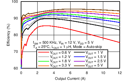
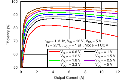
TPS53513 C003_SLUSBN5.png
Figure 1. Efficiency vs Output Current
TPS53513 C005_SLUSBN5.png
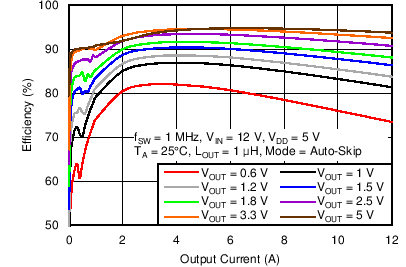
Figure 3. Efficiency vs Output Current
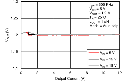
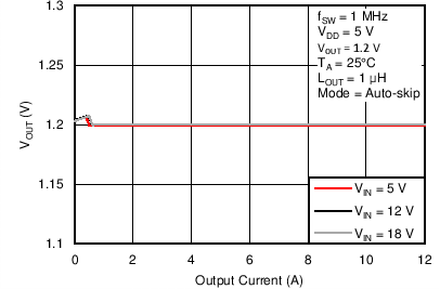
TPS53513 C007_SLUSBN5.png
Figure 5. Output Voltage vs Output Current
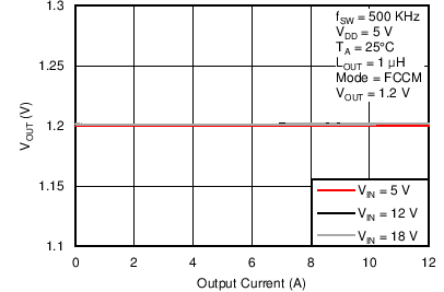
TPS53513 C009_SLUSBN5.png
Figure 7. Output Voltage vs Output Current
TPS53513 C011_SLUSBN5.png
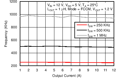
Figure 9. Switching Frequency vs Output Current
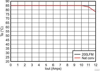
TPS53513 soagraph1.gif
VIN = 12 V Switching frequency = 600kHz
Figure 11. Safe Operating Area, VO = 1.2 V
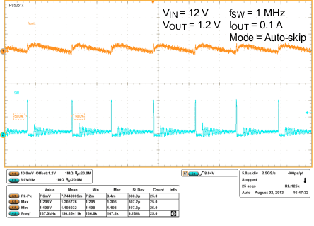
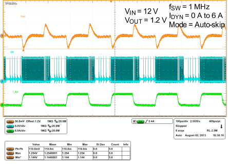
TPS53513 wf1_auto_skip_slusbn5.gif
Figure 13. Auto-Skip Mode Steady-State Operation
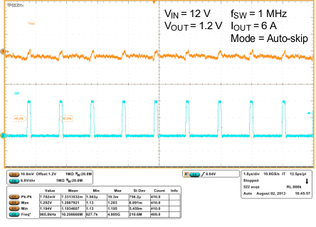
TPS53513 wf3_auto_skip_slusbn5.gif
Figure 15. Auto-Skip Mode Steady-State Operation
TPS53513 wf5_auto_skip_slusbn5.gif
Figure 17. Auto-Skip Mode Steady-State Operation
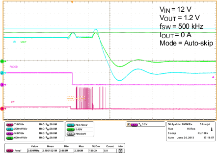
TPS53513 wf7_auto_skip_load_slusbn5.gif
Figure 19. Auto-Skip Mode Load Transient
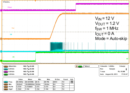
TPS53513 wf9_start_up_slusbn5.gif
Figure 21. Auto‐Skip Mode Start-Up
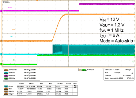
TPS53513 wf11_start_up_slusbn5.gif
Figure 23. Auto‐Skip Mode Start-Up
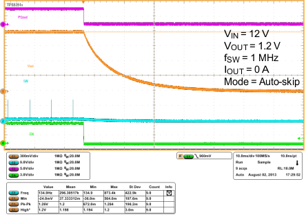
TPS53513 wf13_shutdown_slusbn5.gif
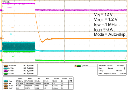
Figure 25. Auto‐Skip Mode Shutdown Operation
TPS53513 wf15_shutdown_slusbn5.gif
Figure 27. Auto‐Skip Mode Shutdown Operation
TPS53513 wf17_shutdown_slusbn5.gif
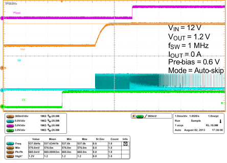
Figure 29. Prebias Operation
TPS53513 wf19_OCP_slusbn5.gif
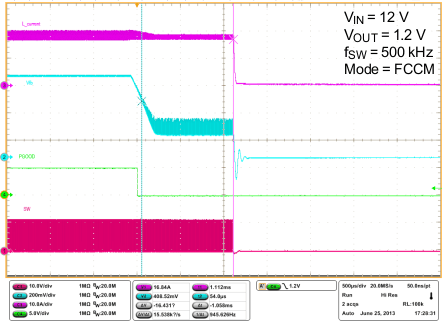
Figure 31. Overcurrent Protection
TPS53513 C004_SLUSBN5.png
Figure 2. Efficiency vs Output Current
TPS53513 C006_SLUSBN5.png
Figure 4. Efficiency vs Output Current
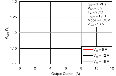
TPS53513 C008_SLUSBN5.png
Figure 6. Output Voltage vs Output Current
TPS53513 C010_SLUSBN5.png
Figure 8. Output Voltage vs Output Current
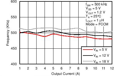
TPS53513 C012_SLUSBN5.png
Figure 10. Switching Frequency vs Output Current
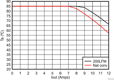
TPS53513 soagraph2.gif
VIN = 12 V Switching frequency = 600kHz
Figure 12. Safe Operating Area, VO = 5 V
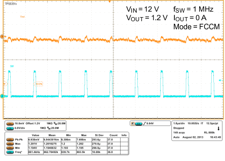
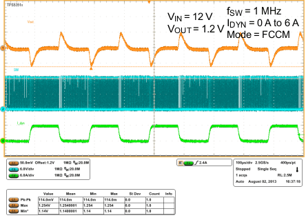
TPS53513 wf2_FCCM_slusbn5.gif
Figure 14. FCCM Steady-State Operation
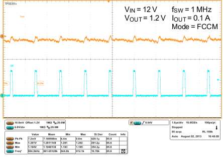
TPS53513 wf4_FCCM_slusbn5.gif
Figure 16. FCCM Steady-State Operation
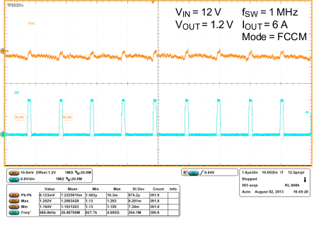
TPS53513 wf6_FCCM_slusbn5.gif
Figure 18. FCCM Steady-State Operation
TPS53513 wf8_fccm_load_slusbn5.gif
Figure 20. FCCM Load Transient
TPS53513 wf10_fccm_load_slusbn5.gif
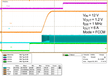
Figure 22. FCCM Start-Up
TPS53513 wf12_fccm_load_slusbn5.gif
Figure 24. FCCM Start-Up
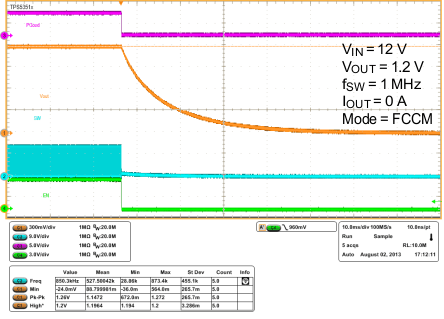
TPS53513 wf14_shutdown_slusbn5.gif
Figure 26. FCCM Shutdown Operation
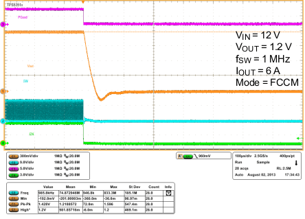
TPS53513 wf16_shutdown_slusbn5.gif
Figure 28. FCCM Shutdown Operation
TPS53513 wf18_ovp_slusbn5.gif
Figure 30. Overvoltage Protection
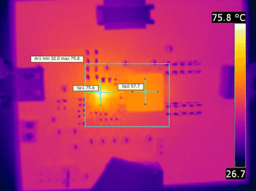
TPS53513 thermal_slusbn5.gif
fSW = 500 kHz VI = 12 V VO = 5 V
IO = 12 A COUT= 10 × 22 µF (1206, 6.3 V, X5R)
SNB = 3 Ω+ 470 pF RBOOT= 0 Ω
Inductor: LOUT = 1 µH 2.1 mΩ (typical)
PCMC135T-1R0MF 12.6 mm × 13.8 mm × 5 mm
Figure 32. SP1: 75.6℃, SP2: 57.7℃ (Inductor)