SLUSCJ3A April 2016 – June 2016 TPS53632G
PRODUCTION DATA.
- 1 Features
- 2 Applications
- 3 Description
- 4 Revision History
- 5 Pin Configuration and Functions
- 6 Specifications
- 7 Timing Requirements
- 8 Switching Characteristics
- 9 Typical Characteristics (Half-Bridge Operation)
-
10Detailed Description
- 10.1 Overview
- 10.2 Functional Block Diagram
- 10.3
Feature Description
- 10.3.1 Current Sensing
- 10.3.2 Load Transients
- 10.3.3 PWM and SKIP Signals
- 10.3.4 5-V, 3.3-V and 1.8-V Undervoltage Lockout (UVLO)
- 10.3.5 Output Undervoltage Protection (UVP)
- 10.3.6 Overcurrent Protection (OCP)
- 10.3.7 Overvoltage Protection
- 10.3.8 Analog Current Monitor, IMON and Corresponding Digital Output Current
- 10.3.9 Addressing
- 10.3.10 I2C Interface Operation
- 10.3.11 Start-Up Sequence
- 10.3.12 Power Good Operation
- 10.3.13 Fault Behavior
- 10.4 Device Functional Modes
- 10.5 Configuration and Programming
- 10.6 Register Maps
-
11Applications and Implementation
- 11.1 Application Information
- 11.2
Typical Application
- 11.2.1
D-CAP+™ Half-Bridge Application
- 11.2.1.1 Design Requirements
- 11.2.1.2
Detailed Design Procedure
- 11.2.1.2.1 Step 1: Select Switching Frequency
- 11.2.1.2.2 Step 2: Set The Slew Rate
- 11.2.1.2.3 Step 3: Determine Inductor Value And Choose Inductor
- 11.2.1.2.4 Step 4: Determine Current Sensing Method
- 11.2.1.2.5 Step 5: DCR Current Sensing
- 11.2.1.2.6 Step 6: Select OCP Level
- 11.2.1.2.7 Step 7: Set the Load-Line Slope
- 11.2.1.2.8 Step 8: Current Monitor (IMON) Setting
- 11.2.1.3 Application Performance Plots
- 11.2.1.4 Loop Compensation for Zero Load-Line
- 11.2.1
D-CAP+™ Half-Bridge Application
- 12Power Supply Recommendations
- 13 Layout
- 14Device and Documentation Support
- 15Mechanical, Packaging, and Orderable Information
9 Typical Characteristics (Half-Bridge Operation)

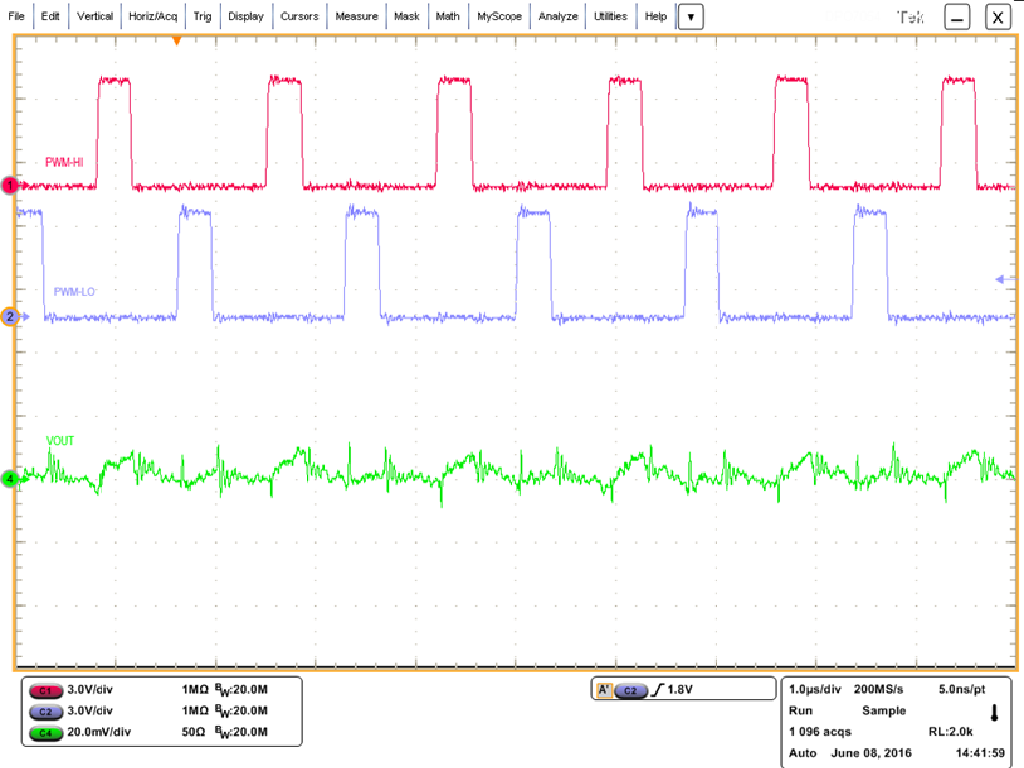
| VIN = 48 V | VOUT = 1 V |
| Load = 1 A |

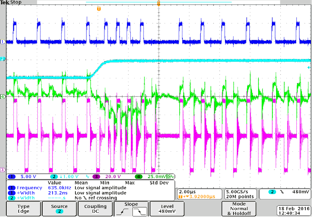
| VIN = 48 V | VOUT = 1 V |
| Load transient from 10 A to 40 A |

| VIN = 48 V | VOUT = 1 V |
| Load = 10 A |

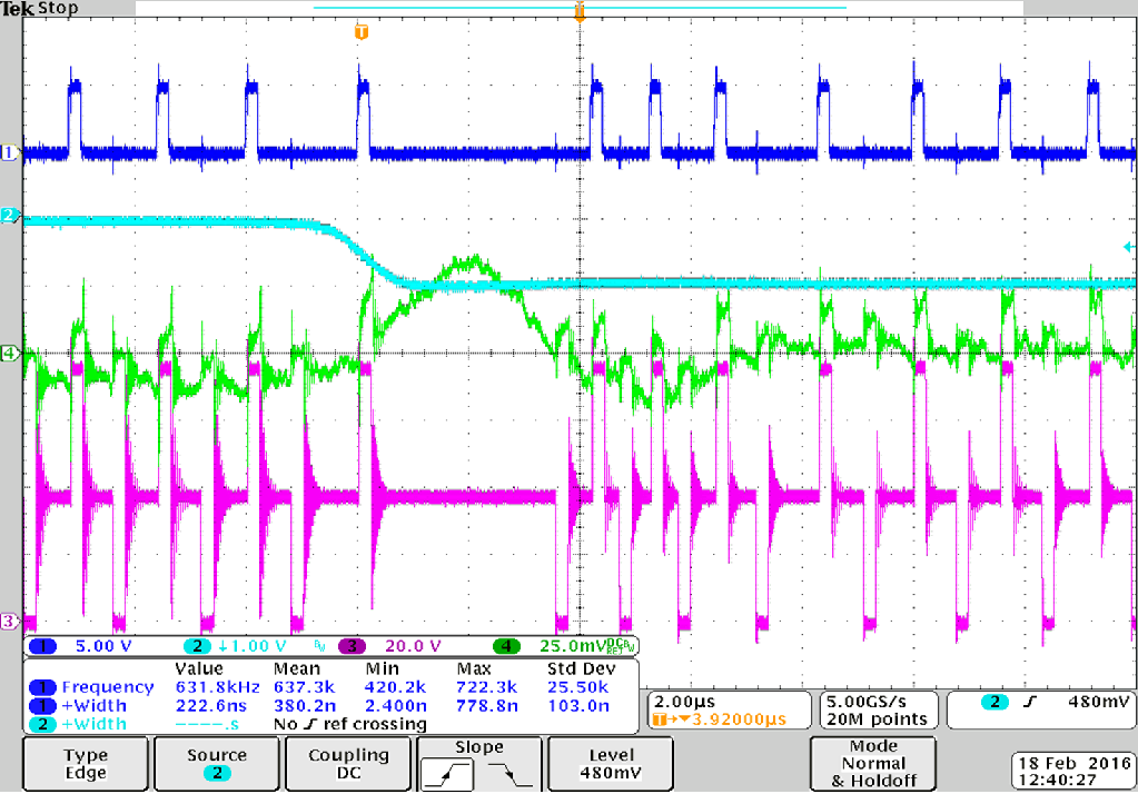
| VIN = 48 V | VOUT = 1 V |
| Load transient from 40 A to 10 A |