ZHCSGE0B June   2017  – January 2019 TPS53681

PRODUCTION DATA.  

  1. 特性
  2. 应用
  3. 说明
    1. 3.1 简化应用
  4. 修订历史记录
  5. Pin Configuration and Functions
    1.     Pin Functions
  6. Specifications
    1. 6.1  Absolute Maximum Ratings
    2. 6.2  ESD Ratings
    3. 6.3  Recommended Operating Conditions
    4. 6.4  Thermal Information
    5. 6.5  Supply: Currents, UVLO, and Power-On Reset
    6. 6.6  References: DAC and VREF
    7. 6.7  Voltage Sense: AVSP and BVSP, AVSN and BVSN
    8. 6.8  Telemetry
    9. 6.9  Input Current Sensing
    10. 6.10 Programmable Loadline Settings
    11. 6.11 Current Sense and Calibration
    12. 6.12 Logic Interface Pins: AVR_EN, AVR_RDY, BVR_EN, BVR_RDY, RESET, VR_FAULT, VR_HOT
    13. 6.13 I/O Timing
    14. 6.14 PMBus Address Setting
    15. 6.15 Overcurrent Limit Thresholds
    16. 6.16 Switching Frequency
    17. 6.17 Slew Rate Settings
    18. 6.18 Ramp Selections
    19. 6.19 Dynamic Integration and Undershoot Reduction
    20. 6.20 Boot Voltage and TMAX Settings
    21. 6.21 Protections: OVP and UVP
    22. 6.22 Protections: ATSEN and BTSEN Pin Voltage Levels and Fault
    23. 6.23 PWM: I/O Voltage and Current
    24. 6.24 Dynamic Phase Add and Drop
    25. 6.25 Typical Characteristics
  7. Detailed Description
    1. 7.1 Overview
    2. 7.2 Functional Block Diagram
    3. 7.3 Feature Description
      1. 7.3.1 Phase Interleaving and PWM Operation
        1. 7.3.1.1 Setting the Load-Line (DROOP)
        2. 7.3.1.2 Load Transitions
          1. 7.3.1.2.1 VID Table
        3. 7.3.1.3 Temperature and Fault Sensing
        4. 7.3.1.4 AutoBalance™ Current Sharing
        5. 7.3.1.5 Phase Configuration for Channel B
        6. 7.3.1.6 RESET Function
    4. 7.4 Device Functional Modes
    5. 7.5 Programming
      1. 7.5.1  PMBus Connections
      2. 7.5.2  PMBus Address Selection
      3. 7.5.3  Supported Commands
      4. 7.5.4  Commonly Used PMBus Commands
      5. 7.5.5  Voltage, Current, Power, and Temperature Readings
        1. 7.5.5.1 (88h) READ_VIN
          1. Table 6. READ_VIN Register Field Descriptions
        2. 7.5.5.2 (89h) READ_IIN
          1. Table 7. READ_IIN Register Field Descriptions
        3. 7.5.5.3 (8Bh) READ_VOUT
          1. Table 8. READ_VOUT Register Field Descriptions
        4. 7.5.5.4 (8Ch) READ_IOUT
          1. Table 9. READ_IOUT Register Field Descriptions
        5. 7.5.5.5 (8Dh) READ_TEMPERATURE_1
          1. Table 10. READ_TEMPERATURE_1 Register Field Descriptions
        6. 7.5.5.6 (96h) READ_POUT
          1. Table 11. READ_POUT Register Field Descriptions
        7. 7.5.5.7 (97h) READ_PIN
          1. Table 12. READ_PIN Register Field Descriptions
        8. 7.5.5.8 (D4h) MFR_SPECIFIC_04
          1. Table 13. MFR_SPECIFIC_04 Register Field Descriptions
      6. 7.5.6  Input Current Sense and Calibration
        1. 7.5.6.1 Measured Input Current Calibration
        2. 7.5.6.2 (DAh) MFR_SPECIFIC_10
          1. Table 15. MFR_SPECIFIC_10 Register Field Descriptions
        3. 7.5.6.3 (DCh) MFR_SPECIFIC_12
          1. Table 17. MFR_SPECIFIC_12 Register Field Descriptions
      7. 7.5.7  Output Current Sense and Calibration
        1. 7.5.7.1 Reading Individual Phase Currents
          1. 7.5.7.1.1 Reading Total Current
          2. 7.5.7.1.2 Calibrating Current Measurements
        2. 7.5.7.2 (38h) IOUT_CAL_GAIN
          1. Table 20. IOUT_CAL_GAIN Register Field Descriptions
        3. 7.5.7.3 (39h) IOUT_CAL_OFFSET
          1. Table 22. IOUT_CAL_OFFSET Register Field Descriptions
      8. 7.5.8  Output Voltage Margin Testing
        1. 7.5.8.1 (01h) OPERATION
          1. Table 25. OPERATION Register Field Descriptions
        2. 7.5.8.2 (21h) VOUT_COMMAND
          1. Table 26. VOUT_COMMAND Register Field Descriptions
        3. 7.5.8.3 (26h) VOUT_MARGIN_LOW
          1. Table 27. VOUT_MARGIN_LOW Register Field Descriptions
        4. 7.5.8.4 (25h) VOUT_MARGIN_HIGH
          1. Table 28. VOUT_MARGIN_HIGH Register Field Descriptions
      9. 7.5.9  Loop Compensation
        1. 7.5.9.1 (D7h) MFR_SPECIFIC_07
          1. Table 29. MFR_SPECIFIC_07 Register Field Descriptions
        2. 7.5.9.2 (28h) VOUT_DROOP
          1. Table 34. VOUT_DROOP Register Field Descriptions
      10. 7.5.10 Converter Protection and Response
      11. 7.5.11 Output Overvoltage Protection and Response
        1. 7.5.11.1 (40h) VOUT_OV_FAULT_LIMIT
          1. Table 37. VOUT_OV_FAULT_LIMIT Register Field Descriptions
        2. 7.5.11.2 (41h) VOUT_OV_FAULT_RESPONSE
          1. Table 38. VOUT_OV_FAULT_RESPONSE Register Field Descriptions
      12. 7.5.12 Maximum Allowed Output Voltage Setting
        1. 7.5.12.1 (24h) VOUT_MAX
          1. Table 39. VOUT_MAX Register Field Descriptions
      13. 7.5.13 Output Undervoltage Protection and Response
        1. 7.5.13.1 (44h) VOUT_UV_FAULT_LIMIT
          1. Table 40. VOUT_UV_FAULT_LIMIT Register Field Descriptions
        2. 7.5.13.2 (45h) VOUT_UV_FAULT_RESPONSE
          1. Table 41. VOUT_UV_FAULT_RESPONSE Register Field Descriptions
      14. 7.5.14 Minimum Allowed Output Voltage Setting
        1. 7.5.14.1 (2Bh) VOUT_MIN
          1. Table 42. VOUT_MIN Register Field Descriptions
      15. 7.5.15 Output Overcurrent Protection and Response
        1. 7.5.15.1 (46h) IOUT_OC_FAULT_LIMIT
          1. Table 43. IOUT_OC_FAULT_LIMIT Register Field Descriptions
        2. 7.5.15.2 (4Ah) IOUT_OC_WARN_LIMIT
          1. Table 44. IOUT_OC_WARN_LIMIT Register Field Descriptions
        3. 7.5.15.3 (47h) IOUT_OC_FAULT_RESPONSE
          1. Table 45. IOUT_OC_FAULT_RESPONSE Register Field Descriptions
      16. 7.5.16 Input Under-Voltage Lockout (UVLO)
        1. 7.5.16.1 (35h) VIN_ON
          1. Table 46. VIN_ON Register Field Descriptions
      17. 7.5.17 Input Over-Voltage Protection and Response
        1. 7.5.17.1 (55h) VIN_OV_FAULT_LIMIT
          1. Table 48. VIN_OV_FAULT_LIMIT Register Field Descriptions
        2. 7.5.17.2 (56h) VIN_OV_FAULT_RESPONSE
          1. Table 49. VIN_OV_FAULT_RESPONSE Register Field Descriptions
      18. 7.5.18 Input Undervoltage Protection and Response
        1. 7.5.18.1 (59h) VIN_UV_FAULT_LIMIT
          1. Table 50. VIN_UV_FAULT_LIMIT Register Field Descriptions
        2. 7.5.18.2 (5Ah) VIN_UV_FAULT_RESPONSE
          1. Table 52. VIN_UV_FAULT_RESPONSE Register Field Descriptions
      19. 7.5.19 Input Overcurrent Protection and Response
        1. 7.5.19.1 (5Bh) IIN_OC_FAULT_LIMIT
          1. Table 53. IIN_OC_FAULT_LIMIT Register Field Descriptions
        2. 7.5.19.2 (5Dh) IIN_OC_WARN_LIMIT
          1. Table 55. IIN_OC_FAULT_LIMIT Register Field Descriptions
        3. 7.5.19.3 (5Ch) IIN_OC_FAULT_RESPONSE
          1. Table 57. IIN_OC_FAULT_LIMIT Register Field Descriptions
      20. 7.5.20 Over-Temperature Protection and Response
        1. 7.5.20.1 (4Fh) OT_FAULT_LIMIT
          1. Table 58. OT_FAULT_LIMIT Register Field Descriptions
        2. 7.5.20.2 (51h) OT_WARN_LIMIT
          1. Table 59. OT_WARN_LIMIT Register Field Descriptions
        3. 7.5.20.3 (50h) OT_FAULT_RESPONSE
          1. Table 60. OT_FAULT_RESPONSE Register Field Descriptions
      21. 7.5.21 Dynamic Phase Shedding (DPS)
        1. 7.5.21.1 (DEh) MFR_SPECIFIC_14
          1. Table 61. MFR_SPECIFIC_14 Register Field Descriptions
        2. 7.5.21.2 (DFh) MFR_SPECIFIC_15
          1. Table 63. MFR_SPECIFIC_15 Register Field Descriptions
      22. 7.5.22 NVM Programming
      23. 7.5.23 NVM Security
        1. 7.5.23.1 (FAh) MFR_SPECIFIC_42
          1. Table 64. MFR_SPECIFIC_42 Register Field Descriptions
      24. 7.5.24 Black Box Recording
        1. 7.5.24.1 (D8h) MFR_SPECIFIC_08
          1. Table 65. MFR_SPECIFIC_08 Register Field Descriptions
      25. 7.5.25 Board Identification and Inventory Tracking
        1. 7.5.25.1 (9Ah) MFR_MODEL
          1. Table 67. MFR_MODEL Register Field Descriptions
        2. 7.5.25.2 (9Bh) MFR_REVISION
          1. Table 68. MFR_REVISION Register Field Descriptions
        3. 7.5.25.3 (9Dh) MFR_DATE
          1. Table 69. MFR_DATE Register Field Descriptions
      26. 7.5.26 Status Reporting
        1. 7.5.26.1 (78h) STATUS_BYTE
          1. Table 70. STATUS_BYTE Register Field Descriptions
        2. 7.5.26.2 (79h) STATUS_WORD
          1. Table 71. STATUS_WORD Register Field Descriptions
        3. 7.5.26.3 (7Ah) STATUS_VOUT
          1. Table 72. STATUS_VOUT Register Field Descriptions
        4. 7.5.26.4 (7Bh) STATUS_IOUT
          1. Table 73. STATUS_IOUT Register Field Descriptions
        5. 7.5.26.5 (7Ch) STATUS_INPUT
          1. Table 74. STATUS_INPUT Register Field Descriptions
        6. 7.5.26.6 (7Dh) STATUS_TEMPERATURE
          1. Table 75. STATUS_TEMPERATURE Register Field Descriptions
        7. 7.5.26.7 (7Eh) STATUS_CML
          1. Table 76. STATUS_CML Register Field Descriptions
        8. 7.5.26.8 (80h) STATUS_MFR_SPECIFIC
          1. Table 77. STATUS_MFR_SPECIFIC Register Field Descriptions
  8. Applications, Implementation, and Layout
    1. 8.1 Application Information
    2. 8.2 Typical Application
      1. 8.2.1 6-phase, 0.9-V, 300-A Application and 2-phase 0.8-V, 90-A Application
        1. 8.2.1.1 Schematic
        2. 8.2.1.2 Design Requirements
        3. 8.2.1.3 Detailed Design Procedure
          1. 8.2.1.3.1 Choose Inductor
          2. 8.2.1.3.2 Select the Per-Phase Valley Current Limit
          3. 8.2.1.3.3 Set the Maximum Temperature Level (TMAX)
          4. 8.2.1.3.4 Set USR Thresholds to Improve Load Transient Performance
        4. 8.2.1.4 Inductor DCR and Shunt Current Sensing Design for Input Power
          1. 8.2.1.4.1 Compensation Design
          2. 8.2.1.4.2 Set PMBus Addresses
        5. 8.2.1.5 Application Performance Plots
  9. Power Supply Recommendations
  10. 10Layout
    1. 10.1 Layout Guidelines
      1. 10.1.1 Device Guidelines
      2. 10.1.2 Power Stage Guidelines
    2. 10.2 Layout Examples
  11. 11器件和文档支持
    1. 11.1 接收文档更新通知
    2. 11.2 社区资源
    3. 11.3 商标
    4. 11.4 静电放电警告
    5. 11.5 术语表
  12. 12机械、封装和可订购信息

封装选项

机械数据 (封装 | 引脚)
散热焊盘机械数据 (封装 | 引脚)
订购信息

AutoBalance™ Current Sharing

The basic mechanism for current sharing is to sense the average phase current, then adjust the pulse width of each phase to equalize the current in each phase as shown in Figure 10. The PWM comparator (not shown) starts a pulse when the feedback voltage meets the reference. The VIN voltage charges Ct(on) through Rt(on). The pulse terminates when the voltage at Ct(on) matches the on-time reference, which normally equals the DAC voltage (VDAC).

The circuit operates in the following fashion. First assume that the 1-µs averaged value from each phase current are equal. In this case, the PWM modulator terminates at VDAC, and the normal pulse width is delivered to the system. If instead, I1 > IAVG, then an offset is subtracted from VDAC, and the pulse width for Phase 1 is shortened to reduce the phase current in Phase 1 for balancing. If I1 < IAVG, then a longer pulse is generated to increase the phase current in Phase 1 to achieve current balancing.
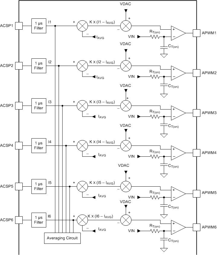
TPS53681 autobalance_ishare_sluscn6.gifFigure 10. AutoBalance Current Sharing Circuit Detail