ZHCSFG9A August 2016 – August 2016 TPS54116-Q1
PRODUCTION DATA.
- 1 特性
- 2 应用
- 3 说明
- 4 修订历史记录
- 5 Pin Configuration and Functions
- 6 Specifications
-
7 Detailed Description
- 7.1 Overview
- 7.2 Functional Block Diagram
- 7.3
Feature Description
- 7.3.1 Fixed Frequency PWM Control
- 7.3.2 Bootstrap Voltage (BOOT) and Low Dropout Operation
- 7.3.3 Error Amplifier
- 7.3.4 Voltage Reference and Adjusting the Output Voltage
- 7.3.5 Enable and Adjusting Undervoltage Lockout
- 7.3.6 Soft Start and Tracking
- 7.3.7 Start-up into Pre-Biased Output
- 7.3.8 Power Good
- 7.3.9 Sequencing
- 7.3.10 Constant Switching Frequency and Timing Resistor (RT/SYNC)
- 7.3.11 Buck Overcurrent Protection
- 7.3.12 Overvoltage Transient Protection
- 7.3.13 VTT Sink and Source Regulator
- 7.3.14 VTTREF
- 7.3.15 Thermal Shutdown
- 7.4 Device Functional Modes
-
8 Application and Implementation
- 8.1 Application Information
- 8.2
Typical Application
- 8.2.1 Design Requirements
- 8.2.2
Detailed Design Procedure
- 8.2.2.1 Switching Frequency
- 8.2.2.2 Output Inductor Selection
- 8.2.2.3 Output Capacitor
- 8.2.2.4 Input Capacitor
- 8.2.2.5 Soft Start Capacitor
- 8.2.2.6 Undervoltage Lock Out Set Point
- 8.2.2.7 Bootstrap Capacitor
- 8.2.2.8 Power Good Pullup
- 8.2.2.9 ILIM Resistor
- 8.2.2.10 Output Voltage and Feedback Resistors Selection
- 8.2.2.11 Compensation
- 8.2.2.12 LDOIN Capacitor
- 8.2.2.13 VTTREF Capacitor
- 8.2.2.14 VTT Capacitor
- 8.2.3 Application Curves
- 9 Power Supply Recommendations
- 10Layout
- 11器件和文档支持
- 12机械、封装和可订购信息
10 Layout
10.1 Layout Guidelines
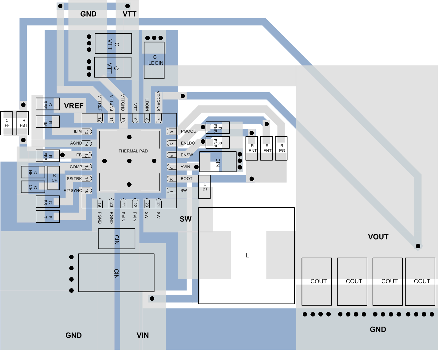
Layout is a critical portion of good power supply design. There are several signal paths that conduct fast changing currents or voltages that can interact with stray inductance or parasitic capacitance to generate noise or degrade the power supplies performance. Guidelines are as follows. See Figure 64 for a PCB layout example.
- The input bypass capacitor for PVIN to PGND should be placed as close as possible to the TPS54116-Q1 with short and wide connections to minimize parasitic inductance.
- The input bypass capacitor for AVIN should be placed as close as possible to the TPS54116-Q1 with a short return to the AGND pin. This capacitor and pin should also be tied to the input voltage before the PVIN bypass capacitors to limit the switching noise from PVIN.
- The output capacitor for VTT to VTTGND should be placed as close as possible to the TPS54116-Q1 with short and wide connections to minimize parasitic inductance and resistance. Too much parasitic inductance and resistance can affect the stability of the high performance VTT LDO.
- The VTTSNS pin should be connected tothe VTT output capacitors as a seperate trace from the high current VTT power trace. If sensing the voltage at the pont of the load is required, it is recommended to also attach the output capacitors at that point while still minimizing parasitic inductance and resistance.
- The input bypass capacitor for LDOIN to VTTGND should be placed as close as possible to the TPS54116-Q1 with short and wide connections to minimize parasitic inductance. This capacitor is used to supply the transient current to the VTT output.
- The VDDQSNS pin should be routed as a separate trace from the high current VDDQ trace and connect near the point of regulation for VDDQ.
- The top of the FB resistor divider should be routed as a separate trace from the high current VDDQ trace and connect near the the point of regulation for VDDQ.
- The analog control circuits should have a return path to the quiet AGND and not overlap with the noisey PGND. Sensitive pins containing analog control circuits are RT/SYNC, SS/TRK, COMP, FB, ILIM, and VTTREF. It is important to minimize the length of the traces connected to the RT/SYNC, COMP, FB and ILIM pins.
- The PGND pins, AGND and VTTGND pin should be tied directly to the power pad under the IC to provide a low impedance connection between the pins.
- The BOOT capacitor should connect directly between the BOOT and SW pins.
- The SW pin should be routed to the output inductor with a short and wide trace to minimize capacitive coupling.
- The thermal pad should be connected to any internal PCB ground planes using multiple vias directly under the IC. For operation at full rated load, the top side ground area and bottom side ground area along with any additional internal ground planes must provide adequate heat dissipating area. For best thermal performance minimize cuts in the bottom side ground copper.
- Additional vias can be used to connect the top side ground area to the internal planes near the input and output capacitors for the buck converter and VTT LDO.
The additional external components can be placed approximately as shown. It may be possible to obtain acceptable performance with alternate PCB layouts, however this layout has been shown to produce good results and is meant as a guideline.
10.2 Layout Example
 Figure 64. PCB Layout Example