| SUPPLY VOLTAGE (AVIN and PVIN PINS) |
|
AVIN and PVIN operating |
|
2.95 |
|
6 |
V |
|
AVIN internal UVLO threshold |
AVIN rising |
|
2.7 |
2.8 |
V |
|
AVIN internal UVLO hysteresis |
|
|
0.05 |
0.12 |
V |
|
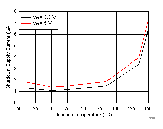
Iq shutdown |
V(ENSW) = V(ENLDO) = 0 V, V(VDDQSNS) = 1.8 V, TJ = 25°C |
|
1 |
3.5 |
µA |
|
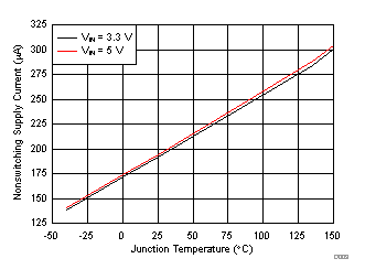
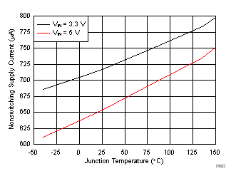
Iq operating — LDO and buck enabled |
V(ENSW) = V(ENLDO) = V(AVIN) = 5 V, V(FB) = 0.7 V, V(VDDQSNS) = 1.8 V, TJ = 25°C |
|
650 |
800 |
µA |
|
Iq operating — LDO enabled, buck disabled |
V(ENLDO) = V(AVIN) = 5 V, V(ENSW) = 0 V, V(VDDQSNS) = 1.8 V, TJ = 25°C |
|
190 |
300 |
µA |
|
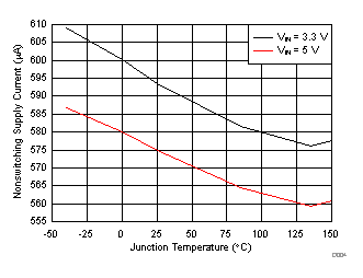
Iq operating — LDO disabled, buck enabled |
V(ENSW) = V(AVIN) = 5 V, V(ENLDO) = 0 V, V(FB) = 0.7 V, V(VDDQSNS) = 1.8 V, TJ = 25°C |
|
570 |
700 |
µA |
| ENABLE (ENSW and ENLDO PINS) |
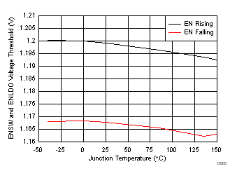
| VENRISING |
ENLDO rising threshold |
ENLDO voltage ramping up |
|
1.20 |
|
V |
| VENFALLING |
ENLDO falling threshold |
ENLDO voltage ramping down |
|
1.17 |
|
|
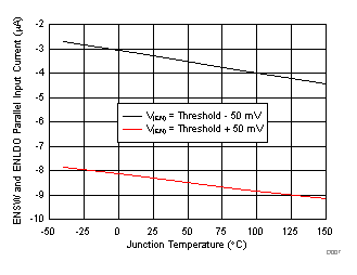
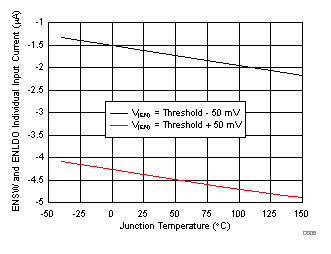
ENLDO input current above voltage threshold |
V(ENLDO) = Enable threshold + 50 mV |
|
-4.4 |
|
µA |
| Ip |
ENLDO input current below voltage threshold |
V(ENLDO) = Enable threshold - 50 mV |
|
-1.7 |
|
| Ih |
ENLDO hysteresis current |
|
|
-2.7 |
|
| VENRISING |
ENSW rising threshold |
ENSW voltage ramping up |
|
1.20 |
|
V |
| VENFALLING |
ENSW falling threshold |
ENSW voltage ramping down |
|
1.17 |
|
|
ENSW input current above voltage threshold |
V(ENSW) = Enable threshold + 50 mV |
|
-4.4 |
|
µA |
| Ip |
ENSW input current below voltage threshold |
V(ENSW) = Enable threshold - 50 mV |
|
-1.7 |
|
| Ih |
ENSW hysteresis current |
|
|
-2.7 |
|
|
Input current above voltage threshold with ENLDO and ENSW connected |
V(ENLDO) = V(ENSW) = Enable threshold + 50 mV |
|
-8.5 |
|
µA |
|
Input current below voltage threshold with ENLDO and ENSW connected |
V(ENLDO) = V(ENSW) = Enable threshold - 50 mV |
|
-3.4 |
|
µA |
|
Hysteresis current with ENLDO and ENSW connected |
|
|
-5.1 |
|
µA |
| VOLTAGE REFERENCE AND ERROR AMPLIFIER (FB AND COMP PINS) |
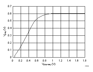
| VREF |
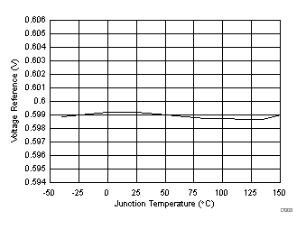
Voltage Reference |
|
0.594 |
0.6 |
0.606 |
V |
|
FB pin input current |
|
|
7 |
|
nA |
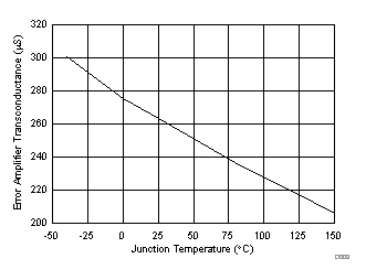
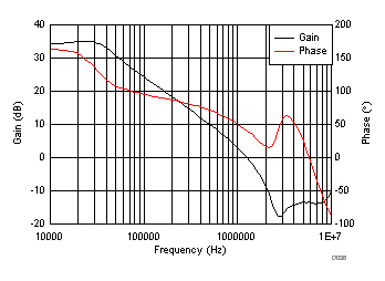
| gmEA |
Error Amp transconductance (gm) |
-2 µA < I(COMP) < 2 µA, V(COMP) = 1 V |
|
260 |
360 |
µS |
|
Error Amp source/sink |
V(COMP) = 1 V, V(FB) = 100 mV overdrive |
|
22 |
|
µA |
| MOSFETS AND POWER STAGE (SW AND BOOT PINS) |
|
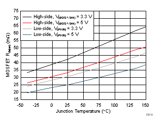
High side switch resistance |
V(BOOT-SW) = 5 V |
|
33 |
66 |
mΩ |
| V(BOOT-SW) = 3.3 V |
|
42 |
84 |
|
Low side switch resistance |
V(PVIN) = 5 V |
|
25 |
50 |
mΩ |
| V(PVIN) = 3.3 V |
|
30 |
60 |
|
BOOT-SW UVLO |
V(PVIN) = 2.95 V |
|
2.2 |
|
V |
|
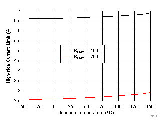
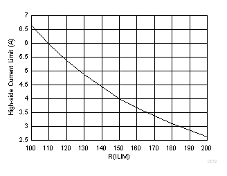
High-side FET current limit |
V(PVIN) = 6V, R(ILIM) = 100k |
5.2 |
6.6 |
8.2 |
A |
|
High-side FET current limit |
V(PVIN) = 6V, R(ILIM) = 200k |
1.5 |
3 |
3.8 |
A |
|
Low-side FET reverse current limit |
|
2 |
4.5 |
|
A |
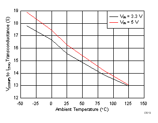
| gmPS |
V(COMP) to I(SW)peak transconductance |
R(ILIM) = 100k |
|
16 |
|
A/V |
|
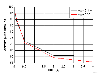
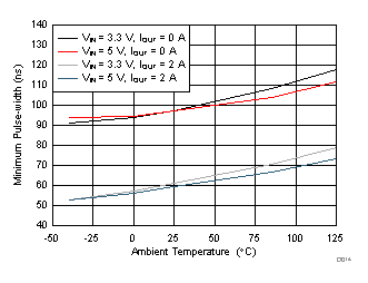
Minimum pulse width |
Measured at 50% points on V(SW), IOUT = 2 A |
|
60 |
|
ns |
|
Minimum pulse width |
Measured at 50% points V(SW), V(PVIN) = 5 V, IOUT = 0 A, TJ = -40°C to 125°C |
|
100 |
125 |
ns |
|
Minimum off-time |
Prior to skipping off pulses, IOUT = 2 A |
|
60 |
|
ns |
| TIMING RESISTOR AND EXTERNAL CLOCK (RT/SYNC PIN) |
|
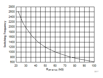
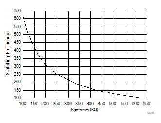
Switching frequency range using RT mode |
|
100 |
|
2500 |
kHz |
|
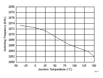
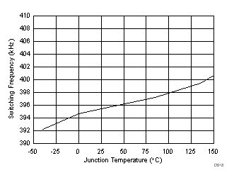
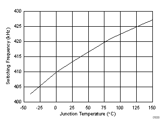
Switching frequency |
R(RT/SYNC) = 150 kΩ |
370 |
400 |
430 |
kHz |
| R(RT/SYNC) = 27 kΩ |
1910 |
2070 |
2230 |
kHz |
| V(RT/SYNC) > 2.2 V or V(RT/SYNC) < 0.35 V |
340 |
420 |
480 |
kHz |
|
Switching frequency range using SYNC mode |
|
100 |
|
2500 |
kHz |
|
Minimum SYNC input pulse width |
|
10 |
|
ns |
|
RT/SYNC high threshold |
|
|
1.5 |
2.2 |
V |
|
RT/SYNC low threshold |
|
0.35 |
0.4 |
|
V |
|
RT/SYNC rising edge to SW rising edge delay |
fSW = 500 kHz |
30 |
45 |
80 |
ns |
|
RT to SYNC lock in time |
R(RT/SYNC) = 150 kΩ |
|
55 |
|
µs |
|
SYNC to RT lock in time |
|
|
60 |
|
µs |
|
Internal RT to SYNC lock in time |
Logic high or logic low at RT/SYNC to SYNC signal |
|
55 |
|
µs |
|
SYNC to internal RT lock in time |
SYNC signal to logic high or logic low at RT/SYNC |
|
60 |
|
µs |
| SOFT START AND TRACKING (SS/TRK PIN) |
| VSSTHR |
SS voltage threshold |
|
|
0.15 |
|
V |
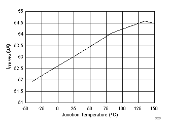
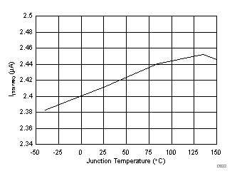
| ISS |
Charge Current |
V(SS/TRK) < VSSTHR |
|
47 |
|
µA |
| V(SS/TRK) > VSSTHR |
1.5 |
2.4 |
3.2 |
µA |
|
SS/TRK to FB matching |
V(SS/TRK) = 0.3 V |
|
60 |
|
mV |
|
SS/TRK to reference crossover |
98% normal |
|
0.85 |
1 |
V |
|
SS/TRK discharge voltage (overload) |
V(FB) = 0 V |
|
120 |
|
mV |
|
SS/TRK discharge voltage (fault) |
V(FB) = 0 V |
|
5 |
|
mV |
|
SS/TRK discharge current (overload) |
V(FB) = 0 V, V(SS/TRK) = 0.4 V |
|
160 |
|
µA |
|
SS/TRK discharge current (AVIN UVLO, ENSW low, thermal fault) |
V(AVIN) = 5 V, V(SS/TRK) = 0.4 V |
|
760 |
|
µA |
| POWER GOOD (PGOOD PIN) |
|
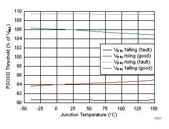
Threshold |
V(FB) falling (fault) |
|
91 |
95 |
% VREF |
| V(FB) rising (good) |
|
94 |
|
| V(FB) rising (fault) |
105 |
109 |
|
| V(FB) falling (good) |
|
106 |
|
|
Hysteresis |
V(FB) falling and rising |
|
3 |
|
|
Output high leakage |
V(FB) = VREF, V(PGOOD) = 5.5 V |
|
5 |
125 |
nA |
|
On resistance |
V(AVIN) = 2.95 V |
|
85 |
170 |
Ω |
|
Minimum V(AVIN) for valid output |
V(PGOOD) < 0.5 V, I(PGOOD) = 100 µA |
|
1.3 |
1.7 |
V |
| TERMINATION REGULATOR INPUTS (VLDOIN AND VDDQSNS PINS) |
|
V(LDOIN) Operating |
|
|
3.5 |
V |
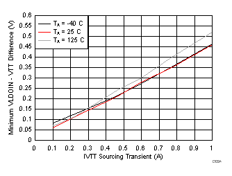
| VDO |
DC V(LDOIN) – V(VTT) dropout |
1.2 V < V(VDDQSNS) < 2.5 V, I(VTT) = 0.5 A, V(VTT) = V(VTTREF) - 40 mV |
|
0.15 |
V |
| VDO |
DC V(LDOIN) – V(VTT) dropout |
1.2 V < V(VDDQSNS) < 2.5 V, I(VTT) = 1.5 A, V(VTT) = V(VTTREF) - 40 mV |
|
0.45 |
V |
|
VLDOIN supply current |
V(LDOIN) = 1.8 V, TJ = 25°C |
|
1 |
µA |
|
VDDQSNS input current |
V(VDDQSNS) = 1.8 V |
|
39 |
46 |
µA |
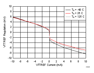
| VTTREF OUTPUT (VTTREF PIN) |
| V(VTTREF) |
VTTREF output voltage |
|
|
V(VDDQSNS)/2 |
|
V |
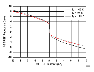
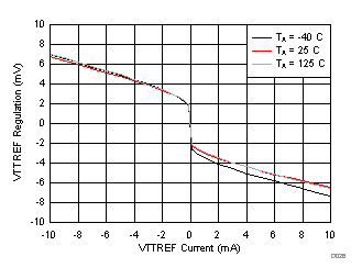
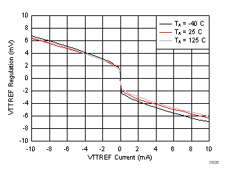
| V(VTTREF)TOL |
VTTREF output voltage difference from V(VDDQSNS)/2 |
|I(VTTREF)| < 10 mA, V(VDDQSNS) = 1.8 V |
-18 |
|
18 |
mV |
| |I(VTTREF)| < 10 mA, V(VDDQSNS) = 1.5 V |
-15 |
|
15 |
| |I(VTTREF)| < 10 mA, V(VDDQSNS) = 1.2 V |
-15 |
|
15 |
| |I(VTTREF)| < 5 mA, V(VDDQSNS) = 1.2 V |
-12 |
|
12 |
| I(VTTREF)SRC |
VTTREF source current limit |
V(VDDQSNS) = 1.8 V, V(VTTREF) = 0 V |
10 |
18 |
|
mA |
| I(VTTREF)SNK |
VTTREF sink current limit |
V(VDDQSNS) = 0 V, V(VTTREF) = 1.8 V |
10 |
19 |
|
mA |
| I(VTTREF)DIS |
VTTREF discharge current |
TJ = 25°C, V(VTTREF) = 0.5V, V(ENLDO) = 0 V |
0.9 |
1.1 |
|
mA |
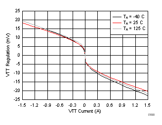
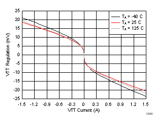
| VTT OUTPUT (VTT PIN) |
| V(VTT) |
VTT output voltage |
|
|
V(VTTREF) |
|
V |
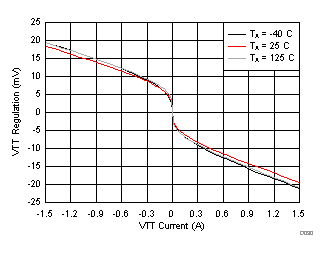
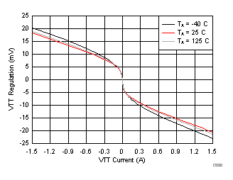
| V(VTT)TOL |
VTT output voltage tolerance to VTTREF |
|I(VTT)|≤ 10 mA, 1.2 V ≤ V(VDDQSNS) ≤ 1.8 V |
-20 |
|
20 |
mV |
| |I(VTT)|≤ 1 A, 1.2 V ≤ V(VDDQSNS) ≤ 1.8 V |
-30 |
|
30 |
| |I(VTT)|≤ 1.5 A, 1.2 V ≤ V(VDDQSNS) ≤ 1.8 V |
-40 |
|
40 |
| I(VTT)SRC |
VTT source current limit |
V(VDDQSNS) = 1.8 V, V(VTT) = V(VTTSNS) = 0.7 V |
1.5 |
2.5 |
|
A |
| I(VTT)SNK |
VTT sink current limit |
V(VDDQSNS) = 1.8 V, V(VTT) = V(VTTSNS) = 1.1 V |
1.5 |
2.5 |
|
A |
| I(VTTSNS)BIAS |
VTTSNS input bias current |
|
-0.1 |
|
0.1 |
µA |
| I(VTT)DIS |
VTT discharge current |
TJ = 25°C, V(VTT) = 0.5 V, V(ENLDO) = 0 V |
4.8 |
6 |
|
mA |
| THERMAL SHUTDOWN |
|
Thermal shutdown temperature |
|
|
175 |
|
℃ |
|
Thermal shutdown hysteresis |
|
|
16 |
|
℃ |
