ZHCSFG9A August 2016 – August 2016 TPS54116-Q1
PRODUCTION DATA.
- 1 特性
- 2 应用
- 3 说明
- 4 修订历史记录
- 5 Pin Configuration and Functions
- 6 Specifications
-
7 Detailed Description
- 7.1 Overview
- 7.2 Functional Block Diagram
- 7.3
Feature Description
- 7.3.1 Fixed Frequency PWM Control
- 7.3.2 Bootstrap Voltage (BOOT) and Low Dropout Operation
- 7.3.3 Error Amplifier
- 7.3.4 Voltage Reference and Adjusting the Output Voltage
- 7.3.5 Enable and Adjusting Undervoltage Lockout
- 7.3.6 Soft Start and Tracking
- 7.3.7 Start-up into Pre-Biased Output
- 7.3.8 Power Good
- 7.3.9 Sequencing
- 7.3.10 Constant Switching Frequency and Timing Resistor (RT/SYNC)
- 7.3.11 Buck Overcurrent Protection
- 7.3.12 Overvoltage Transient Protection
- 7.3.13 VTT Sink and Source Regulator
- 7.3.14 VTTREF
- 7.3.15 Thermal Shutdown
- 7.4 Device Functional Modes
-
8 Application and Implementation
- 8.1 Application Information
- 8.2
Typical Application
- 8.2.1 Design Requirements
- 8.2.2
Detailed Design Procedure
- 8.2.2.1 Switching Frequency
- 8.2.2.2 Output Inductor Selection
- 8.2.2.3 Output Capacitor
- 8.2.2.4 Input Capacitor
- 8.2.2.5 Soft Start Capacitor
- 8.2.2.6 Undervoltage Lock Out Set Point
- 8.2.2.7 Bootstrap Capacitor
- 8.2.2.8 Power Good Pullup
- 8.2.2.9 ILIM Resistor
- 8.2.2.10 Output Voltage and Feedback Resistors Selection
- 8.2.2.11 Compensation
- 8.2.2.12 LDOIN Capacitor
- 8.2.2.13 VTTREF Capacitor
- 8.2.2.14 VTT Capacitor
- 8.2.3 Application Curves
- 9 Power Supply Recommendations
- 10Layout
- 11器件和文档支持
- 12机械、封装和可订购信息
7 Detailed Description
7.1 Overview
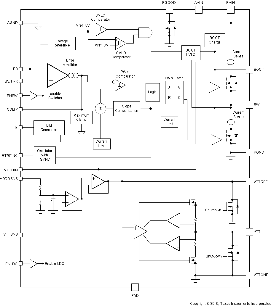
The TPS54116-Q1 is a 6-V, 4-A, synchronous step-down (buck) converter with two integrated N-channel MOSFETs and integrated 1-A sink/source double data rate (DDR) VTT termination regulator with a VTTREF buffed reference output.
To improve the performance during line and load transients the buck converter implements a constant frequency, peak current mode control which reduces output capacitance and simplifies external frequency compensation design. The wide switching frequency range of 100 kHz to 2500 kHz allows for efficiency and size optimization when selecting the output filter components. The switching frequency is adjusted using a resistor to ground on the RT/SYNC pin. The RT/SYNC pin can also be used to synchronize the power switch turn on to the rising edge of an external clock. The switching frequency can be set using an internal resistor by pulling the RT/SYNC below the low threshold or above the high threshold.
The TPS54116-Q1 has a typical default start-up voltage of 2.7 V. The ENSW pin can be used to enable the buck converter and the ENLDO pin can be used to enable VTT and VTTREF. The ENSW and ENLDO pins have internal pullup current sources that can be used to adjust the input voltage under voltage lockout (UVLO) with two external resistors. In addition, the pullup current provides a default condition when the ENSW or ENLDO pin is floating for the device to operate. The total operating current for the TPS54116-Q1 is typically 650 µA when not switching and under no load. When the device is disabled, the supply current is less than 3.5 µA.
The integrated 33-mΩ and 25-mΩ MOSFETs allow for high-efficiency power supply designs with continuous output currents up to 4 amperes. The TPS54116-Q1 reduces the external component count by integrating the boot recharge diode. The bias voltage for the integrated high-side MOSFET is supplied by a capacitor between the BOOT and SW pins. The boot capacitor voltage is monitored by an UVLO circuit and turns off the high-side MOSFET when the voltage falls below the BOOT-SW UVLO threshold. This BOOT circuit allows the TPS54116-Q1 to operate approaching 100% duty cycle. The output voltage can be stepped down to as low as the 0.60-V reference.
The TPS54116-Q1 features monotonic start-up under prebias conditions. The low-side FET turns on for a short time period every cycle before the output voltage reaches the prebiased voltage. This ensures the boot capacitor has enough charge to turn on the top FET when the output voltage reaches the prebiased voltage.
The TPS54116-Q1 has a power good comparator (PGOOD) with 3% hysteresis. Excessive output overvoltage transients are minimized by taking advantage of the overvoltage power good comparator. When the regulated output voltage (as sensed by the FB voltage) is greater than 109% of the nominal voltage, the overvoltage comparator is activated, and the high-side MOSFET is turned off and masked from turning on until the output voltage is lower than 106%.
The SS/TRK (soft-start or tracking) pin is used to minimize inrush currents or provide power supply sequencing during power up. A small value capacitor should be coupled to the pin for soft-start. The SS/TRK pin is discharged before the output power up to ensure a repeatable restart after an over temperature fault, UVLO fault or disabled condition. To optimize the output startup waveform, two levels of SS/TRK output current are implemented.
The TPS54116-Q1 limits the peak inductor current by sensing the current through the high-side MOSFET with cycle-by-cycle protection. The peak current limit is adjusted using a resistor to ground on the ILIM pin. The reverse current through the low-side MOSFET is also limited.
The 10-mA VTTREF buffered reference uses an internal resistor divider to regulate its output within 49% to 51% of VDDQSNS. The 1-A VTT termination regulates to VTTREF and maintains fast transient response with only 2 × 10-µF ceramic output capacitance. Remote sensing of VTT is used for best regulation. The VTT and VTTREF outputs are discharged when disabled with the AVIN UVLO or with ENLDO.
7.2 Functional Block Diagram
7.3 Feature Description
7.3.1 Fixed Frequency PWM Control
The TPS54116-Q1 uses an adjustable fixed frequency, peak current mode control. The output voltage is compared through external resistors on the FB pin to an internal voltage reference by an error amplifier which drives the COMP pin. An internal oscillator initiates the turn on of the high-side power switch. The error amplifier output is compared to the high-side power switch current. When the power switch current reaches the COMP signal level the high-side power switch is turned off and the low-side power switch is turned on. The COMP pin voltage will increase and decrease as the output current increases and decreases. The device implements a current limit by clamping the internal COMP signal.
An internal ramp is used to provide slope compensation to prevent sub-harmonic oscillations. The peak inductor current limit is constant over the full duty cycle range.
7.3.2 Bootstrap Voltage (BOOT) and Low Dropout Operation
The TPS54116-Q1 has an integrated boot regulator and requires a small ceramic capacitor between the BOOT and SW pins to provide the gate drive voltage for the high-side MOSFET. The value of the ceramic capacitor should be 0.1 µF. A ceramic capacitor with an X7R or X5R grade dielectric is recommended because of the stable characteristics over temperature and voltage.
To improve dropout, the TPS54116-Q1 is designed to operate at 100% duty cycle as long as the BOOT-SW voltage is greater than 2.2 V. The high-side MOSFET is turned off using an UVLO circuit, allowing for the low-side MOSFET to conduct, when the BOOT-SW voltage drops below 2.2 V. Because the supply current sourced from the BOOT pin is low, the high-side MOSFET can remain on for more switching cycles than are required to refresh the capacitor, thus the effective duty of the switching regulator is high.
7.3.3 Error Amplifier
The TPS54116-Q1 has a transconductance amplifier for the error amplifier. The error amplifier compares the FB voltage to the lower of the SS/TRK pin voltage or the internal 0.6-V voltage reference. The transconductance (gmEA) of the error amplifier is 260 µA/V during normal operation. During soft-start, the gmEA is reduced to 90 µA/V. The frequency compensation components are added to the COMP pin to ground.
When operating at current limit the COMP pin voltage is clamped to a maximum level to improve response when the load current decreases. When FB is greater than the internal voltage reference or SS/TRK the COMP pin voltage is clamped to a minimum level and the devices enters a high-side skip mode.
7.3.4 Voltage Reference and Adjusting the Output Voltage
The voltage reference system produces a precise ±1% voltage reference over temperature by scaling the output of a temperature stable bandgap circuit. The FB voltage is regulated to the voltage reference. The output voltage is set with a resistor divider from the output node to the FB pin. It is recommended to use divider resistors with 1% tolerance or better. Start with a 10.0 kΩ for the bottom resistor RFBB and use the Equation 1 to calculate RFBT. The maximum recommend resistance value for the bottom resistor is 100 kΩ.
vertical spacer

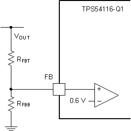 Figure 40. Voltage Divider Circuit
7.3.5 Enable and Adjusting Undervoltage Lockout
The TPS54116-Q1 is enabled when the AVIN pin voltage exceeds 2.7 V and is disabled when it falls below 2.65 V. If an application requires a higher under-voltage lockout (UVLO) or more hysteresis, use the ENSW or ENLDO pins as shown in Figure 41 to adjust the input voltage UVLO by using two external resistors. The EN pin has an internal pull-up current source (Ip) of 1.7 µA that provides the default condition of the TPS54116-Q1 operating when the EN pin floats. Once the EN pin voltage exceeds 1.2 V, an additional 2.7 μA hysteresis current (Ih) is added. When the EN pin is pulled below 1.17 V, the 2.7 μA is removed. This additional current facilitates input voltage hysteresis. It is recommended to use the EN resistors to set the UVLO falling threshold (VSTOP) at 2.65V or higher. The rising threshold (VSTART) should be set to provide enough hysteresis to allow for any input supply variations. Equation 2 can be used to calculate the top resistor in the EN divider and Equation 3 is used to calculate the bottom resistor.
The ENSW and ENLDO can also be tied in parallel. Calculations can be done the same but with the increased EN current of Ip = 3.4 µA and Ih = 5.1 µA.
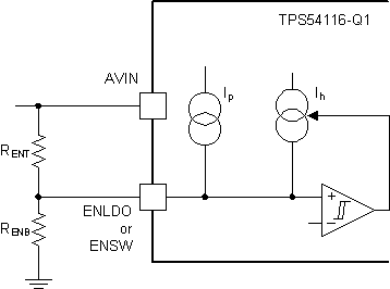 Figure 41. Adjustable Under Voltage Lock Out

vertical spacer

Where:
- Ih = 2.7 µA
- Ip = 1.7 µA
- VENRISING = 1.2 V
- VENFALLING = 1.17 V
7.3.6 Soft Start and Tracking
The TPS54116-Q1 regulates to the lower of the SS/TRK pin and the internal reference voltage. A capacitor on the SS/TRK pin to ground implements a soft start time. Before the SS pin reaches the voltage threshold VSSTHR of 0.15 V, the charge current is about 47 μA. The TPS54116-Q1 internal pull-up current source of 2.4 μA charges the external soft start capacitor after the SS pin voltage exceeds VSSTHR. Equation 4 calculates the required soft start capacitor value where tSS is the desired soft start time for the output voltage to reach 90% its final value in ms and CSS is the required capacitance in nF.
vertical spacer

If during normal operation, AVIN goes below the UVLO, ENSW pin pulled below 1.17 V, or a thermal shutdown event occurs, the TPS54116-Q1 stops switching. When the AVIN goes above UVLO, ENSW is released or pulled high, or a thermal shutdown is exited, then SS/TRK is discharged to below 5 mV before reinitiating a powering up sequence. The FB voltage will follow the SS/TRK pin voltage with a 60 mV offset up to 90% of the internal voltage reference. When the SS/TRK voltage is greater than 90% of the internal reference voltage the offset increases as the effective system reference transitions from the SS/TRK voltage to the internal voltage reference.
When the COMP pin voltage is clamped by the maximum COMP clamp in an overload condition the soft-start pin is discharged to near the FB voltage. When the overload condition is removed, the soft-start circuit controls the recovery from the fault output level to the nominal regulation voltage. At the beginning of recovery a spike in the output voltage may occur as the COMP voltage transitions to the value determined by the loop.
7.3.7 Start-up into Pre-Biased Output
The TPS54116-Q1 features monotonic startup into pre-biased output. The low-side MOSFET turns on for a very short time period every cycle before the output voltage reaches the pre-biased voltage. This ensures the BOOT-SW cap has enough charge to turn on the high-side MOSFET when the output voltage reaches the pre-biased voltage. The low-side MOSFET reverse current protection provides another layer of protection but it should not be reached due to the implemented prebias function.
7.3.8 Power Good
The PGOOD pin is an open-drain output requiring an external pullup resistor to output a high signal. Once the FB pin is between 94% and 106% of the internal voltage reference, the PGOOD pin is de-asserted and the pin floats. A pull up resistor between the values of 10 kΩ and 100 kΩ to a voltage source that is 6 V or less is recommended. The PGOOD is in a defined state once the AVIN input voltage is greater than 1.3 V but with reduced current sinking capability.
The PGOOD pin is pulled low when the FB is lower than 91% or greater than 109% of the nominal internal reference voltage. The PGOOD is also pulled low if AVIN falls below its UVLO, ENSW pin is pulled low or the TPS54116-Q1 enters thermal shutdown.
7.3.9 Sequencing
Many of the common power supply sequencing methods can be implemented using the SS/TRK, ENSW and PGOOD pins. The sequential method can be implemented using an open-drain or collector output of a power on reset pin of another device. An example sequential method is shown in Figure 42. PGOOD is connected to the EN pin on the next power supply, which will enable the second power supply once the first supply reaches regulation.
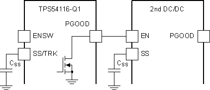 Figure 42. Sequential Startup Example
7.3.10 Constant Switching Frequency and Timing Resistor (RT/SYNC)
The switching frequency of the TPS54116-Q1 is adjustable over a wide range from 100 kHz to 2500 kHz by placing a maximum of 620 kΩ and minimum of 22 kΩ, respectively, on the RT/SYNC pin. Alternatively the RT/SYNC pin can be tied above the high threshold or below the low threshold to use an internal RT resistor to set the switching frequency to 420 kHz. The RT/SYNC is typically 0.5 V and the current through the resistor sets the switching frequency. To determine the timing resistance for a given switching frequency, refer to the curve in Figure 16 and Figure 17 or use Equation 5. For a given RT resistor the nominal switching frequency can be calculated with Equation 6. To reduce the solution size one would typically set the switching frequency as high as possible, but tradeoffs of the supply efficiency, maximum input voltage and minimum controllable on time should be considered. The minimum controllable on time is typically 60 ns at 2-A load current and 100 ns at no load, and will limit the maximum operating input voltage or minimum output voltage.


The RT/SYNC pin can also be used to synchronize the converter to an external system clock. When using the internal RT resistor, the TPS54116-Q1 cannot be synchronized to an external clock. The synchronization frequency range is 100 kHz to 2500 kHz. The rising edge of SW will be synchronized to the rising edge of RT/SYNC. To implement the synchronization feature in a system connect a square wave to the RT/SYNC pin with on-time at least 10 ns. The square wave amplitude at this pin must transition lower than 0.35 V and higher than 2.2 V.
See Figure 43 for synchronizing to a high impedance system clock. See Figure 44 and Figure 45 for synchronizing to a low impedance system clock. A tri-state buffer with its output directly connected to the RT/SYNC pin is the recommended method to accomodate a wide range of external clock frequencies and duty cycles. Alternatively an AC blocking capacitor circuit can be used when synchronizing to frequencies greater than 800 kHz and with clock signals with duty cycle near 50%. When using an AC coupling capacitor to interface with an external clock, RT/SYNC is not actively pulled low by the external clock. As a result the TPS54116-Q1 begins its transition back to RT mode while the external clock is low. When connecting the RT/SYNC pin to the external clock source, it is important to minimize routing connected to the RT/SYNC pin as much as possible to minimize noise sensitivity when operating in RT mode.
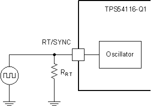 Figure 43. Synchronizing to a High Impedance System Clock
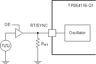 Figure 44. Interfacing to the RT/SYNC Pin with Buffer
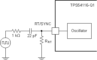 Figure 45. Interfacing to the RT/SYNC Pin with RC
7.3.11 Buck Overcurrent Protection
The TPS54116-Q1 implements current mode control which uses the COMP pin voltage to turn off the high-side MOSFET and turn on the low-side MOSFET on a cycle-by-cycle basis. Each cycle the switch current and the COMP pin voltage are compared, when the peak switch current intersects the COMP voltage the high-side switch is turned off. During overcurrent conditions that pull the output voltage low, the error amplifier will respond by driving the COMP pin high, increasing the switch current. The error amplifier output is clamped internally. This clamp functions as a high-side switch current limit.
A resistor placed from ILIM to AGND sets the peak current limit of the buck converter in the TPS54116-Q1. A 100 kΩ resistor sets it to the maximum value and a 200 kΩ resistor sets it to the minimum value. Any resistor within this range can be used. Figure 12 shows the relationship between peak current limit and ILIM resistor. To determine the resistor value for a target current limit use Equation 7.
vertical spacer

The TPS54116-Q1 also implements low-side current protection by detecting the voltage over the low-side MOSFET. When the converter sinks current through the low-side MOSFET is more than 4.5 A, the control circuit will turn the low-side MOSFET off immediately for the rest of the clock cycle. Under this condition, both the high-side and low-side are off until the start of the next cycle.
7.3.12 Overvoltage Transient Protection
The TPS54116-Q1 incorporates an overvoltage transient protection (OVTP) circuit to minimize voltage overshoot when recovering from output fault conditions or strong unload transients. The OVTP feature minimizes the output overshoot by implementing a circuit to compare the FB pin voltage to OVTP threshold which is 109% of the internal voltage reference. If the FB pin voltage is greater than the OVTP threshold, the high-side MOSFET is disabled preventing current from flowing to the output and minimizing output overshoot. The output voltage can overshoot the 109% threshold as the current in the inductor discharges to 0 A. When the FB voltage drops lower than the OVTP threshold the high-side MOSFET is allowed to turn on the next clock cycle.
7.3.13 VTT Sink and Source Regulator
The TPS54116-Q1 integrates a high-performance, low-dropout (LDO) linear regulator (VTT) that has ultimate fast response to track ½ VDDQSNS within 40 mV at all conditions, and its current capability is 1.5 A peak current for both sink and source directions. Two 10-µF (or greater) ceramic capacitor(s) need to be attached close to the VTT pin for stable operation. X5R grade or better is recommended. To achieve tight regulation with minimum effect of trace resistance, the remote sensing terminal, VTTSNS, should be connected to the positive terminal of the output capacitor(s) as a separate trace from the high current path from the VTT pin.
The device has a dedicated pin, VLDOIN, for VTT power supply to minimize the LDO power dissipation on user application. The minimum VLDOIN voltage is 0.45 V above the ½ VDDQSNS voltage.
7.3.14 VTTREF
The VTTREF pin has a 10 mA sink and source current capability, and regulates to within 49% to 51% of VDDQSNS. A 0.22-µF ceramic capacitor needs to be attached close to the VTTREF terminal for stable operation. X5R grade or better is recommended.
7.3.15 Thermal Shutdown
The device implements an internal thermal shutdown to protect itself if the junction temperature exceeds 175°C. The thermal shutdown has a hysteresis of 16°C. When the junction temperature exceeds thermal trip threshold, thermal shutdown forces the device to stop switching and discharges both VTT and VTTREF. When the die temperature decreases below 159°C, the device reinitiates the power-up sequence by discharging the SS/TRK pin.
7.4 Device Functional Modes
The enable pins and an AVIN UVLO are used to control turn on and turn off of the TPS54116-Q1. The device becomes active when V(AVIN) exceeds the 2.7 V typical UVLO and when either V(ENSW) or V(ENLDO) exceeds 1.20 V typical. The ENSW pin is used to control the turn on and turn off of the buck converter. The ENLDO pin is used to control the turn on and turn off of the VTTREF and VTT outputs of the termination regulator. The ENSW and ENLDO pins both have an internal current source to enable their respective outputs when left floating. Both ENSW and ENLDO need to be pulled low to put the device into a low quiescent current state.