ZHCSI03C September 2009 – April 2018 TPS54318
PRODUCTION DATA.
- 1 特性
- 2 应用
- 3 说明
- 4 修订历史记录
- 5 Pin Configuration and Functions
- 6 Specifications
-
7 Detailed Description
- 7.1 Overview
- 7.2 Functional Block Diagram
- 7.3
Feature Description
- 7.3.1 Fixed Frequency PWM Control
- 7.3.2 Slope Compensation and Output Current
- 7.3.3 Bootstrap Voltage (Boot) and Low Dropout Operation
- 7.3.4 Error Amplifier
- 7.3.5 Voltage Reference
- 7.3.6 Adjusting the Output Voltage
- 7.3.7 Enable and Adjusting Undervoltage Lockout
- 7.3.8 Soft-Start Pin
- 7.3.9 Sequencing
- 7.3.10 Constant Switching Frequency and Timing Resistor (RT/CLK Pin)
- 7.3.11 Overcurrent Protection
- 7.3.12 Frequency Shift
- 7.3.13 Reverse Overcurrent Protection
- 7.3.14 Synchronize Using the RT/CLK Pin
- 7.3.15 Power Good (PWRGD Pin)
- 7.3.16 Overvoltage Transient Protection
- 7.3.17 Thermal Shutdown
- 7.4 Device Functional Modes
-
8 Application and Implementation
- 8.1 Application Information
- 8.2
Typical Application
- 8.2.1 Design Requirements
- 8.2.2
Detailed Design Procedure
- 8.2.2.1 Step One: Select the Switching Frequency
- 8.2.2.2 Step Two: Select the Output Inductor
- 8.2.2.3 Step Three: Choose the Output Capacitor
- 8.2.2.4 Step Four: Select the Input Capacitor
- 8.2.2.5 Step Five: Minimum Load DC COMP Voltage
- 8.2.2.6 Step Six: Choose the Soft-Start Capacitor
- 8.2.2.7 Step Seven: Select the Bootstrap Capacitor
- 8.2.2.8 Step Eight: Undervoltage Lockout Threshold
- 8.2.2.9 Step Nine: Select Output Voltage and Feedback Resistors
- 8.2.2.10 Step 10: Select Loop Compensation Components
- 8.2.2.11 Power Dissipation Estimate
- 8.2.3 Application Curves
- 9 Power Supply Recommendations
- 10Layout
- 11器件和文档支持
- 12机械、封装和可订购信息
7.3.9 Sequencing
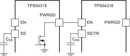
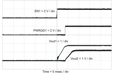
Many of the common power supply sequencing methods can be implemented using the SS, EN and PWRGD pins. The sequential method can be implemented using an open drain or collector output of a power on reset pin of another device. Figure 25 shows the sequential method. The power good is coupled to the EN pin on theTPS54318 device which enables the second power supply once the primary supply reaches regulation.
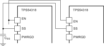
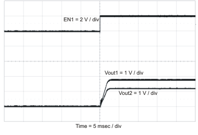
Ratiometric start up can be accomplished by connecting the SS pins together. The regulator outputs ramp up and reach regulation at the same time. When calculating the soft-start time the pull up current source must be doubled in Equation 4. The ratiometric method is shown in Figure 27.
 Figure 25. Sequencial Start-Up Schematic
 Figure 26. Sequential Startup using EN and PWRGD
 Figure 27. Ratiometric Start-Up Schematic
 Figure 28. Ratiometric Start-Up Using Coupled SS Pins