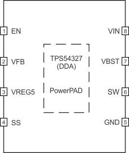
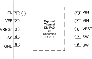
| EN |
1 |
1 |
I |
Enable input control. Active high. |
| VFB |
2 |
2 |
I |
Converter feedback input. Connect to output voltage with feedback resistor divider. |
| VREG5 |
3 |
3 |
O |
5.5 V power supply output. A capacitor (typical 1 µF) should be connected to GND. VREG5 is not active when EN is low. |
| SS |
4 |
4 |
O |
Soft-start control. An external capacitor should be connected to GND. |
| GND |
5 |
5 |
G |
Ground pin. Power ground return for switching circuit. Connect sensitive SS and VFB returns to GND at a single point. |
| SW |
6 |
6, 7 |
O |
Switch node connection between high-side NFET and low-side NFET. |
| VBST |
7 |
8 |
I |
Supply input for the high-side FET gate drive circuit. Connect 0.1µF capacitor between VBST and SW pins. An internal diode is connected between VREG5 and VBST. |
| VIN |
8 |
9, 10 |
P |
Input voltage supply pin. |
| PowerPAD |
Back side |
— |
G |
PowerPAD of the package. Must be soldered to achieve appropriate dissipation. Must be connected to GND. |
| Exposed thermal pad |
— |
Back side |
G |
Thermal pad of the package. PGND power ground return of internal low-side FET. Must be soldered to achieve appropriate dissipation. |

