ZHCSM42C may 2020 – april 2023 TPS543320
PRODUCTION DATA
- 1
- 1 特性
- 2 应用
- 3 说明
- 4 Revision History
- 5 Pin Configuration and Functions
- 6 Specifications
-
7 Detailed Description
- 7.1 Overview
- 7.2 Functional Block Diagram
- 7.3
Feature Description
- 7.3.1 VIN Pins and VIN UVLO
- 7.3.2 Enable and Adjustable UVLO
- 7.3.3 Adjusting the Output Voltage
- 7.3.4 Switching Frequency Selection
- 7.3.5 Switching Frequency Synchronization to an External Clock
- 7.3.6 Ramp Amplitude Selection
- 7.3.7 Soft Start and Prebiased Output Start-Up
- 7.3.8 Mode Pin
- 7.3.9 Power Good (PGOOD)
- 7.3.10 Current Protection
- 7.3.11 Output Overvoltage and Undervoltage Protection
- 7.3.12 Overtemperature Protection
- 7.3.13 Output Voltage Discharge
- 7.4 Device Functional Modes
-
8 Application and Implementation
- 8.1 Application Information
- 8.2
Typical Applications
- 8.2.1
3.3-V Output, 1.0-MHz Application
- 8.2.1.1 Design Requirements
- 8.2.1.2
Detailed Design Procedure
- 8.2.1.2.1 Switching Frequency
- 8.2.1.2.2 Output Inductor Selection
- 8.2.1.2.3 Output Capacitor
- 8.2.1.2.4 Input Capacitor
- 8.2.1.2.5 Adjustable Undervoltage Lockout
- 8.2.1.2.6 Output Voltage Resistors Selection
- 8.2.1.2.7 Bootstrap Capacitor Selection
- 8.2.1.2.8 BP5 Capacitor Selection
- 8.2.1.2.9 PGOOD Pullup Resistor
- 8.2.1.2.10 Current Limit Selection
- 8.2.1.2.11 Soft-Start Time Selection
- 8.2.1.2.12 Ramp Selection and Control Loop Stability
- 8.2.1.2.13 MODE Pin
- 8.2.1.3 Application Curves
- 8.2.2 1.8-V Output, 1.5-MHz Application
- 8.2.1
3.3-V Output, 1.0-MHz Application
- 8.3 Power Supply Recommendations
- 8.4 Layout
- 9 Device and Documentation Support
- 10Mechanical, Packaging, and Orderable Information
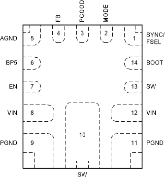
5 Pin Configuration and Functions
 Figure 5-1
14-Pin VQFN-HR
RPY Package
(Top View)
Table 5-1 Pin Functions
| Pin | Type | Description | |
|---|---|---|---|
| Name | NO. | ||
| SYNC/FSEL | 1 | I | Frequency select and external clock synchronization. A resistor to ground sets the switching frequency of the device. An external clock can also be applied to this pin to synchronize the switching frequency. |
| MODE | 2 | I | A resistor to ground selects the current limit, soft-start rate, and PWM ramp amplitude. |
| PGOOD | 3 | O | Open-drain power-good indicator |
| FB | 4 | I | Feedback pin for output voltage regulation. Connect this pin to the midpoint of a resistor divider to set the output voltage. |
| AGND | 5 | — | Ground return for internal analog circuits |
| BP5 | 6 | O | Internal 4.5-V regulator output. Bypass this pin with a 2.2-μF capacitor to AGND. |
| EN | 7 | I | Enable pin. Float to enable, enable or disable with an external signal, or adjust the input undervoltage lockout with a resistor divider. |
| VIN | 8, 12 | I | Input power to the power stage. Low impedance bypassing of these pins to PGND is critical. A 10-nF to 100-nF capacitor from each VIN to PGND close to IC is required. |
| PGND | 9, 11 | — | Ground return for the power stage. This pin is internally connected to the source of the low-side MOSFET. |
| SW | 10 | O | Switch node of the converter. Connect this pin to the output inductor. |
| SW | 13 | O | Return path for the internal high-side MOSFET gate driver bootstrap capacitor. Connect a capacitor from BOOT to this pin. The SW pins are connected internally. |
| BOOT | 14 | I | Supply for the internal high-side MOSFET gate driver. Connect a capacitor from this pin to SW. |