ZHCSA92G August   2012  – June 2018 TPS54360

PRODUCTION DATA.  

  1. 特性
  2. 应用
  3. 说明
    1.     Device Images
      1.      简化电路原理图
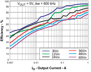
      2.      效率与负载电流间的关系
  4. 修订历史记录
  5. Pin Configuration and Functions
    1.     Pin Functions
  6. Specifications
    1. 6.1 Absolute Maximum Ratings
    2. 6.2 ESD Ratings
    3. 6.3 Recommended Operating Conditions
    4. 6.4 Thermal Information
    5. 6.5 Electrical Characteristics
    6. 6.6 Timing Requirements
    7. 6.7 Typical Characteristics
  7. Detailed Description
    1. 7.1 Overview
    2. 7.2 Functional Block Diagram
    3. 7.3 Feature Description
      1. 7.3.1  Fixed Frequency PWM Control
      2. 7.3.2  Slope Compensation Output Current
      3. 7.3.3  Pulse Skip Eco-mode
      4. 7.3.4  Low Dropout Operation and Bootstrap Voltage (BOOT)
      5. 7.3.5  Error Amplifier
      6. 7.3.6  Adjusting the Output Voltage
      7. 7.3.7  Enable and Adjusting Undervoltage Lockout
      8. 7.3.8  Internal Soft-Start
      9. 7.3.9  Constant Switching Frequency and Timing Resistor (RT/CLK) Terminal)
      10. 7.3.10 Accurate Current Limit Operation and Maximum Switching Frequency
      11. 7.3.11 Synchronization to RT/CLK Terminal
      12. 7.3.12 Overvoltage Protection
      13. 7.3.13 Thermal Shutdown
      14. 7.3.14 Small Signal Model for Loop Response
      15. 7.3.15 Simple Small Signal Model for Peak Current Mode Control
      16. 7.3.16 Small Signal Model for Frequency Compensation
    4. 7.4 Device Functional Modes
      1. 7.4.1 Operation with VIN = < 4.5 V (Minimum VIN)
      2. 7.4.2 Operation with EN Control
      3. 7.4.3 Alternate Power Supply Topologies
        1. 7.4.3.1 Inverting Power
        2. 7.4.3.2 Split-Rail Power Supply
  8. Application and Implementation
    1. 8.1 Application Information
    2. 8.2 Typical Application
      1. 8.2.1 Design Requirements
      2. 8.2.2 Detailed Design Procedure
        1. 8.2.2.1  Custom Design with WEBENCH® Tools
        2. 8.2.2.2  Selecting the Switching Frequency
        3. 8.2.2.3  Output Inductor Selection (LO)
        4. 8.2.2.4  Output Capacitor
        5. 8.2.2.5  Catch Diode
        6. 8.2.2.6  Input Capacitor
        7. 8.2.2.7  Bootstrap Capacitor Selection
        8. 8.2.2.8  Undervoltage Lockout Set Point
        9. 8.2.2.9  Output Voltage and Feedback Resistors Selection
        10. 8.2.2.10 Minimum VIN
        11. 8.2.2.11 Compensation
        12. 8.2.2.12 Discontinuous Conduction Mode and Eco-mode Boundary
        13. 8.2.2.13 Power Dissipation Estimate
      3. 8.2.3 Application Curves
  9. Power Supply Recommendations
  10. 10Layout
    1. 10.1 Layout Guidelines
    2. 10.2 Layout Example
      1. 10.2.1 Estimated Circuit Area
  11. 11器件和文档支持
    1. 11.1 文档支持
      1. 11.1.1 使用 WEBENCH® 工具定制设计方案
    2. 11.2 接收文档更新通知
    3. 11.3 社区资源
    4. 11.4 商标
    5. 11.5 静电放电警告
  12. 12机械、封装和可订购信息

封装选项

机械数据 (封装 | 引脚)
散热焊盘机械数据 (封装 | 引脚)
订购信息

Application Curves

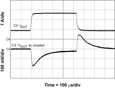
TPS54360 ac_G001_lvsbb4.gif
Figure 35. Load Transient
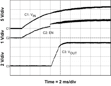
TPS54360 ac_G003_lvsbb4.gif
Figure 37. Start-up With VIN
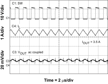
TPS54360 ac_G005_lvsbb4.gif
Figure 39. Output Ripple CCM
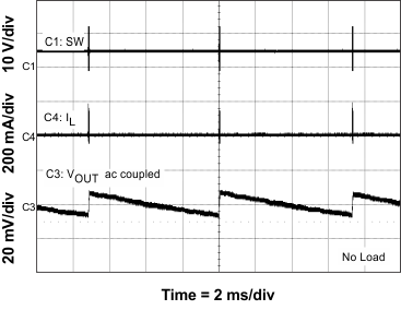
TPS54360 ac_G007_lvsbb4.gif
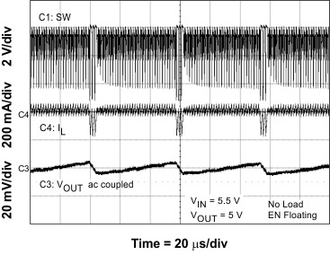
Figure 41. Output Ripple PSM
TPS54360 ac_G009_lvsbb4.gif
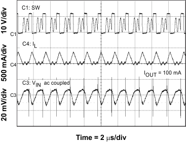
Figure 43. Input Ripple DCM
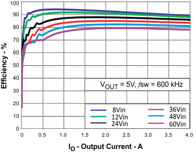
TPS54360 eff_vs_load_lvsbb4.gif
Figure 45. Efficiency vs Load Current
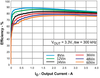
TPS54360 eff_vs_3.3V_load_lvsbb4.gif
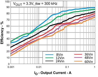
Figure 47. Efficiency vs Load Current
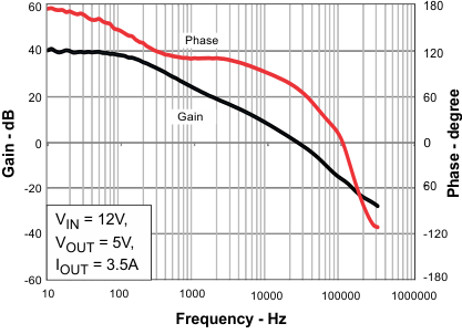
TPS54360 gain_phase_lvsbb4.gif
Figure 49. Overall Loop Frequency Response
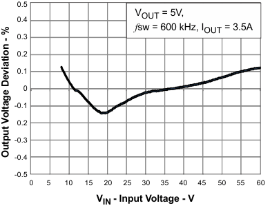
TPS54360 reg_vs_Vi_lvsbb4.gif
Figure 51. Regulation vs Input Voltage
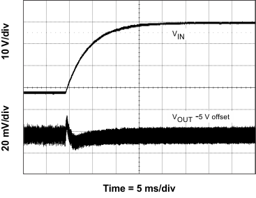
TPS54360 ac_G002_lvsbb4.gif
Figure 36. Line Transient (8 V to 40 V)
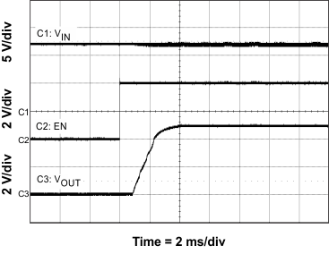
TPS54360 ac_G004_lvsbb4.gif
Figure 38. Start-up With EN
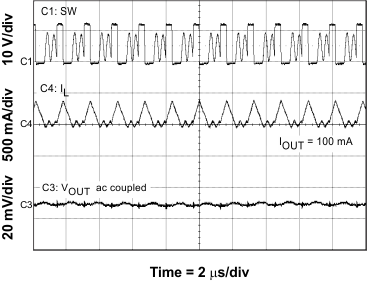
TPS54360 ac_G006_lvsbb4.gif
Figure 40. Output Ripple DCM
TPS54360 ac_G008_lvsbb4.gif
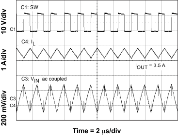
Figure 42. Input Ripple CCM
TPS54360 ac_G010_lvsbb4.gif
Figure 44. Low Dropout Operation
TPS54360 light_load_eff_vs_current_lvsbb4.gif
Figure 46. Light Load Efficiency
TPS54360 light_load_eff_vs_3.3Vcurrent_lvsbb4.gif
Figure 48. Light Load Efficiency
TPS54360 reg_vs_load_lvsbb4.gif
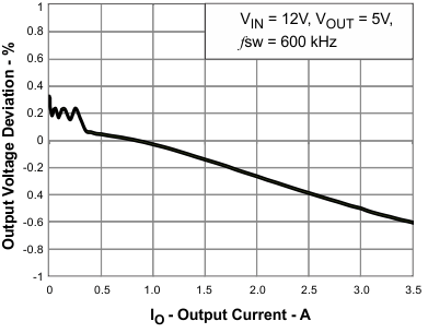
Figure 50. Regulation vs Load Current