ZHCSGJ0B May 2017 – March 2018 TPS543B20
PRODUCTION DATA.
- 1 特性
- 2 应用
- 3 说明
- 4 修订历史记录
- 5 Device Comparison Table
- 6 Pin Configuration and Functions
- 7 Specifications
-
8 Detailed Description
- 8.1 Overview
- 8.2 Functional Block Diagram
- 8.3 Feature Description
- 8.4
Device Functional Modes
- 8.4.1 Soft-Start Operation
- 8.4.2 Input and VDD Undervoltage Lockout (UVLO) Protection
- 8.4.3 Power Good and Enable
- 8.4.4 Voltage Reference
- 8.4.5 Prebiased Output Start-up
- 8.4.6 Internal Ramp Generator
- 8.4.7 Switching Frequency
- 8.4.8 Clock Sync Point Selection
- 8.4.9 Synchronization and Stackable Configuration
- 8.4.10 Dual-Phase Stackable Configurations
- 8.4.11 Operation Mode
- 8.4.12 API/BODY Brake
- 8.4.13 Sense and Overcurrent Protection
- 8.4.14 Output Overvoltage and Undervoltage Protection
- 8.4.15 Overtemperature Protection
- 8.4.16 RSP/RSN Remote Sense Function
- 8.4.17 Current Sharing
- 8.4.18 Loss of Synchronization
-
9 Application and Implementation
- 9.1 Application Information
- 9.2
Typical Application: TPS543B20 Stand-alone Device
- 9.2.1 Design Requirements
- 9.2.2 Detailed Design Procedure
- 9.2.3 Application Curves
- 9.3 System Example
- 10Power Supply Recommendations
- 11Layout
- 12器件和文档支持
- 13机械、封装和可订购信息
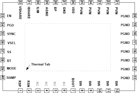
6 Pin Configuration and Functions
RVF Package
40-Pin LQFN
Top View

Pin Functions
| PIN | I/O/P(1) | DESCRIPTION | |
|---|---|---|---|
| NO. | NAME | ||
| 1 | RSP | I | The positive input of the remote sense amplifier. Connect RSP pin to the output voltage at the load. For multi-phase configuration, the remote sense amplifier is not needed for slave devices. |
| 2 | RSN | I | The negative input of the remote sense amplifier. Connect RSN pin to the ground at load side. For multi-phase configuration, the remote sense amplifier is not needed for slave devices. |
| 3 – 6 | NC | Not connected | |
| 7 | BOOT | I | Bootstrap pin for the internal flying high-side driver. Connect a typical 100-nF capacitor from this pin to SW. To reduce the voltage spike at SW, a BOOT resistor with a value between 1 Ω to 10 Ω may be placed in series with the BOOT capacitor to slow down turnon of the high-side FET. |
| 8 – 12 | SW | B | Output of converted power. Connect this pin to the output Inductor. |
| 13 – 20 | PGND | G | These ground pins are connected to the return of the internal low-side MOSFET |
| 21 – 25 | PVIN | I | Input power to the power stage. Low impedance bypassing of these pins to PGND is critical. A 10-nF to 100-nF capacitor from PVIN to PGND close to IC is required. |
| 26 | VDD | I | Controller power supply input |
| 27 | GND | G | Ground return for the controller. This pin should be directly connected to the thermal pad on the PCB board. A 10-nF to 100-nF capacitor from PVIN to GND close to IC is required. |
| 28 | BP | O | Output of the 5 V on board regulator. This regulator powers the driver stage of the controller and must be bypassed with a minimum of 2.2 µF to the thermal pad (power stage ground, that is, GND). Low impedance bypassing of this pin to PGND is critical. |
| 29 | AGND | G | GND return for internal analog circuits. |
| 30 | ILIM | O | Current protection pin; connect a resistor from this pin to AGND sets current limit level. |
| 31 | ISHARE | I | Current sharing signal for multi-phase operation. Float this pin for single phase. |
| 32 | VSHARE | B | Voltage sharing signal for multi-phase operation. Float this pin for single phase. |
| 33 | EN | I | The enable pin turns on the switcher. |
| 34 | PGD | O | Open-drain power-good status signal which provides start-up delay after the FB voltage falls within the specified limits. After the FB voltage moves outside the specified limits, PGOOD goes low. |
| 35 | SYNC | B | For frequency synchronization. This pin can be configured as sync in or sync out by MODE pin and RT pin for master and slave devices. |
| 36 | VSEL | I | Connect a resistor from this pin to AGND to select internal reference voltage. |
| 37 | SS | O | Connect a resistor from this pin to AGND to select soft-start time. |
| 38 | RT | O | Frequency setting pin. Connect a resistor from this pin to AGND to program the switching frequency. This pin also selects sync point for devices in stackable applications |
| 39 | MODE | B | Enable or disable API or body brake function, choose API threshold, also selects the operation mode in stackable applications |
| 40 | RAMP | B | Ramp level selection, with a resistor to AGND to adjust internal loop. |
| – | Thermal Tab | – | Package thermal tab, internally connected to PGND. The thermal tab must have adequate solder coverage for proper operation. |
(1) I = Input, O = Output, B = Bidirectional, P = Supply, G = Ground