ZHCSGK1 July 2017 TPS54424
PRODUCTION DATA.
- 1 特性
- 2 应用
- 3 说明
- 4 修订历史记录
- 5 Pin Configuration and Functions
- 6 Specifications
-
7 Detailed Description
- 7.1 Overview
- 7.2 Functional Block Diagram
- 7.3
Feature Description
- 7.3.1 Fixed Frequency PWM Control
- 7.3.2 Continuous Conduction Mode Operation (CCM)
- 7.3.3 VIN Pins and VIN UVLO
- 7.3.4 Voltage Reference and Adjusting the Output Voltage
- 7.3.5 Error Amplifier
- 7.3.6 Enable and Adjustable UVLO
- 7.3.7 Soft Start and Tracking
- 7.3.8 Safe Start-up into Pre-Biased Outputs
- 7.3.9 Power Good
- 7.3.10 Sequencing (SS/TRK)
- 7.3.11 Adjustable Switching Frequency (RT Mode)
- 7.3.12 Synchronization (CLK Mode)
- 7.3.13 Bootstrap Voltage and 100% Duty Cycle Operation (BOOT)
- 7.3.14 Output Overvoltage Protection (OVP)
- 7.3.15 Overcurrent Protection
- 7.4 Device Functional Modes
-
8 Application and Implementation
- 8.1 Application Information
- 8.2
Typical Application
- 8.2.1 Design Requirements
- 8.2.2
Detailed Design Procedure
- 8.2.2.1 Custom Design With WEBENCH® Tools
- 8.2.2.2 Switching Frequency
- 8.2.2.3 Output Inductor Selection
- 8.2.2.4 Output Capacitor
- 8.2.2.5 Input Capacitor
- 8.2.2.6 Output Voltage Resistors Selection
- 8.2.2.7 Soft-start Capacitor Selection
- 8.2.2.8 Undervoltage Lockout Set Point
- 8.2.2.9 Bootstrap Capacitor Selection
- 8.2.2.10 PGOOD Pull-up Resistor
- 8.2.2.11 Compensation
- 8.2.3 Application Curves
- 9 Power Supply Recommendations
- 10Layout
- 11器件和文档支持
- 12机械、封装和可订购信息
6 Specifications
6.1 Absolute Maximum Ratings
over operating free-air temperature range (unless otherwise noted)(1)| MIN | MAX | UNIT | ||
|---|---|---|---|---|
| Voltage | VIN | –0.3 | 19 | V |
| BOOT | –0.3 | 27 | ||
| BOOT (10 ns transient) | –0.3 | 30 | ||
| BOOT (vs SW) | –0.3 | 7 | ||
| SW | –1 | 20 | ||
| SW (10 ns transient) | –3 | 23 | ||
| EN, SS/TRK, PGOOD, RT/CLK, FB, COMP | –0.3 | 6.5 | ||
| Operating Junction Temperature Range, TJ | -40 | 150 | °C | |
| Storage Temperature Range, TSTG | -55 | 150 | °C | |
6.2 ESD Ratings
| VALUE | UNIT | |||
|---|---|---|---|---|
| V(ESD) | Electrostatic discharge | Human body model (HBM), per ANSI/ESDA/JEDEC JS-001, all pins(1) | ±2000 | V |
| Charged device model (CDM), per JEDEC specification JESD22-C101, all pins(2) | ±500 | |||
6.3 Recommended Operating Conditions
over operating free-air temperature range (unless otherwise noted)| Parameter | MIN | NOM | MAX | UNIT | |
|---|---|---|---|---|---|
| VIN | Input voltage range | 4.5 | 17 | V | |
| VOUT | Output Voltage | 0.6 | 12 | V | |
| IOUT | Output current | 4 | A | ||
| TJ | Operating junction temperature | -40 | 150 | °C | |
| fSW | Switching Frequency (RT mode and PLL mode) | 200 | 1600 | kHz | |
6.4 Thermal Information
| THERMAL METRIC(1) | TPS54424 | UNIT | |
|---|---|---|---|
| RNV | |||
| 18 PINS | |||
| ThetaJA | Junction-to-ambient thermal resistance JEDEC | 57.1 | °C/W |
| ThetaJA | Junction-to-ambient thermal resistance EVM | 34 | °C/W |
| ThetaJCtop | Junction-to-case (top) thermal resistance | 26.3 | °C/W |
| ThetaJB | Junction-to-board thermal resistance | 18.8 | °C/W |
| PsiJT | Junction-to-top characterization parameter | 0.8 | °C/W |
| PsiJB | Junction-to-board characterization parameter | 18.8 | °C/W |
| ThetaJCbot | Junction-to-case (bottom) thermal resistance | 1.2 | °C/W |
6.5 Electrical Characteristics
TJ = -40°C to 150°C, VIN = 4.5 V to 17 V (unless otherwise noted)| PARAMETER | TEST CONDITIONS | MIN | TYP | MAX | UNIT | |
|---|---|---|---|---|---|---|
| INPUT VOLTAGE | ||||||
| UVLO_rise | VIN under-voltage lockout | V(VIN) rising | 4.1 | 4.3 | V | |
| UVLO_fall | V(VIN) falling | 3.7 | 3.9 | V | ||
| UVLO_hys | Hysteresis VIN voltage | 0.2 | V | |||
| Ivin | Operating non-switching supply current | V(EN) = 5 V, V(FB) = 1.5 V | 580 | 800 | µA | |
| Ivin_sdn | Shutdown supply current | V(EN) = 0 V | 3 | 11 | µA | |
| ENABLE | ||||||
| Ven_rise | EN threshold | V(EN) rising | 1.20 | 1.26 | V | |
| Ven_fall | V(EN) falling | 1.1 | 1.15 | V | ||
| Ven_hys | EN pin threshold voltage hysteresis | 50 | mV | |||
| Ip | EN pin sourcing current | V(EN) = 1.1V | 1.2 | µA | ||
| Iph | EN pin sourcing current | V(EN) = 1.3V | 4.8 | µA | ||
| Ih | EN pin hysteresis current | 3.6 | µA | |||
| FB | ||||||
| VFB | Regulated FB voltage | TJ = 25°C | 596 | 600 | 604 | mV |
| 595 | 600 | 605 | mV | |||
| ERROR AMPLIFIER | ||||||
| gmea | Error Amplifier Transconductance (gm) | –2 µA < I(COMP) < 2 µA, V(COMP) = 1 V | 1100 | µA/V | ||
| Error Amplifier DC gain | 80 | dB | ||||
| Icomp_src | Error Amplifier source current | V(FB) = 0 V | 100 | µA | ||
| Icomp_snk | Error Amplifier sink current | V(FB) = 2 V | -100 | µA | ||
| gmps | Power Stage Transconductance | 17 | A/V | |||
| SOFT-START | ||||||
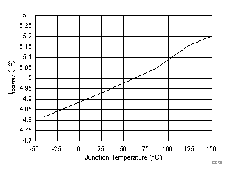
| Iss | Soft-start current | 5 | µA | |||
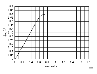
| V(SS/TRK) to V(FB) matching | V(SS/TRK) = 0.4 V | 25 | mV | |||
| MOSFET | ||||||
| Rds(on)_h | High-side switch resistance | TA = 25°C, V(VIN) = 12 V | 14.1 | mΩ | ||
| TA = 25°C, V(VIN) = 4.5 V, V(BOOT-SW) = 4.5 V | 15.9 | mΩ | ||||
| Rds(on)_l | Low-side switch resistance | TA = 25°C, V(VIN) = 12 V | 6.1 | mΩ | ||
| TA = 25°C, V(VIN) = 4.5 V | 6.9 | mΩ | ||||
| BOOT UVLO Falling | 2.2 | 2.6 | V | |||
| CURRENT LIMIT | ||||||
| Ioc_HS_pk | High-side peak current limit | V(VIN) = 12 V | 5.6 | 6.8 | 8.5 | A |
| Ioc_LS_snk | Low-side sinking current limit | V(VIN) = 12 V | -3.4 | A | ||
| Ioc_LS_src | Low-side sourcing current limit | V(VIN) = 12 V | 4.8 | 6.2 | 7.3 | A |
| RT/CLK | ||||||
| VIH | Logic high input voltage | 2 | V | |||
| VIL | Logic low input voltage | 0.8 | V | |||
| PGOOD | ||||||
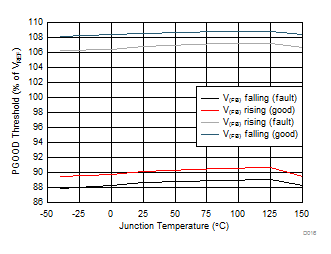
| Power good threshold | V(FB) rising (fault) | 108 | % | |||
| V(FB) falling (good) | 106 | % | ||||
| V(FB) rising (good) | 91 | % | ||||
| V(FB) falling (fault) | 89 | % | ||||
| Ipg_lkg | Leakage current into PGOOD pin when pulled high | V(PGOOD) = 5 V | 5 | nA | ||
| Vpg_low | PGOOD voltage when pulled low | I(PGOOD) = 2 mA | 0.3 | V | ||
| Minimum VIN for valid output | V(PGOOD) < 0.5 V, I(PGOOD) = 4 mA | 0.7 | 1 | V | ||
| Thermal protection | ||||||
| TTRIP | Thermal protection trip point | Temperature Rising | 170 | °C | ||
| THYST | Thermal protection hysteresis | 15 | °C | |||
6.6 Switching Characteristics
TJ = -40°C to 150°C, V(VIN) = 4.5 V to 17 V (unless otherwise noted)| PARAMETER | TEST CONDITIONS | MIN | TYP | MAX | UNIT | |
|---|---|---|---|---|---|---|
| EN | ||||||
| EN to start of switching | 135 | µs | ||||
| PGOOD | ||||||
| Deglitch time PGOOD going high | 272 | Cycles | ||||
| Deglitch time PGOOD going low | 16 | Cycles | ||||
| SW | ||||||
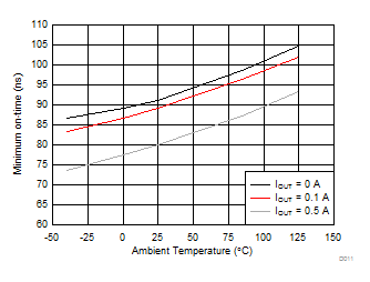
| ton_min | Minimum on time (1) | Measured at 50% to 50% of VIN, L = 1.5 µH, IOUT = 0 A | 90 | 130 | ns | |
| toff_min | Minimum off time (2) | V(BOOT-SW) ≥ 2.6 V | 0 | ns | ||
| RT/CLK | ||||||
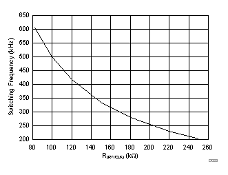
| fsw_min | Minimum switching frequency (RT mode) | R(RT/CLK) = 250 kΩ | 200 | kHz | ||
| Switching frequency (RT mode) | R(RT/CLK) = 100 kΩ | 450 | 500 | 550 | kHz | |
| fsw_max | Maximum switching frequency (RT mode) | R(RT/CLK) = 30.1 kΩ | 1.6 | MHz | ||
| fsw_clk | Switching frequency synchronization range (PLL mode) | 200 | 1600 | kHz | ||
| RT/CLK falling edge to SW rising edge delay (PLL mode) | Measure at 500kHz with RT resistor in series with RT/CLK | 70 | ns | |||
| HICCUP | ||||||
| Wait time before hiccup | 512 | Cycles | ||||
| Hiccup time before restart | 16384 | Cycles | ||||
(1) Characterized. Not production tested.
(2) Specified by design.
6.7 Timing Requirements
TJ = -40°C to 150°C, V(VIN) = 4.5 V to 17 V (unless otherwise noted)| MIN | NOM | MAX | UNIT | |||
|---|---|---|---|---|---|---|
| Minimum synchronization signal pulse width (PLL mode) | 35 | ns | ||||
6.8 Typical Characteristics
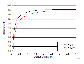
| VOUT = 5 V | fSW = 800 kHz | TA = 25 °C |
| WE 744311220 | L = 2.2 µH | DCR = 11.4 mΩ |
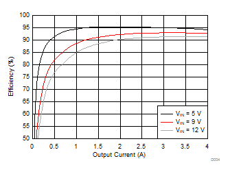
| VOUT = 2.5 V | fSW = 700 kHz | TA = 25 °C |
| WE 744311220 | L = 2.2 µH | DCR = 11.4 mΩ |
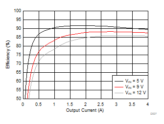
| VOUT = 1.2 V | fSW = 600 kHz | TA = 25 °C |
| WE 74438357012 | L = 1.2 µH | DCR = 13.4 mΩ |
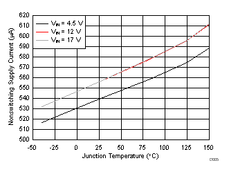
| V(EN) = 5 V | V(FB) = 0.8 V |
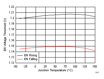
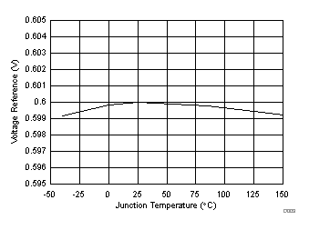
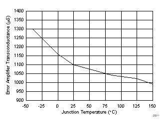
| VIN = 12 V | L = 1.5 µH |
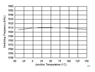
| R(RT/CLK) = 30.1 kΩ |
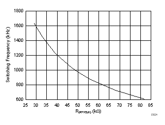
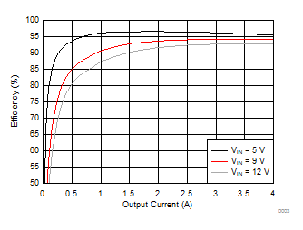
| VOUT = 3.3 V | fSW = 700 kHz | TA = 25 °C |
| WE 744311220 | L = 2.2 µH | DCR = 11.4 mΩ |
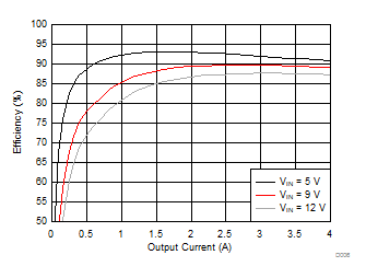
| VOUT = 1.5 V | fSW = 700 kHz | TA = 25 °C |
| WE 74438357018 | L = 1.8 µH | DCR = 18 mΩ |
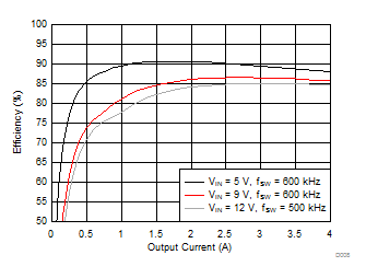
| VOUT = 1.0 V | TA = 25 °C | TA = 25 °C |
| WE 74438357012 | L = 1.2 µH | DCR = 13.4 mΩ |
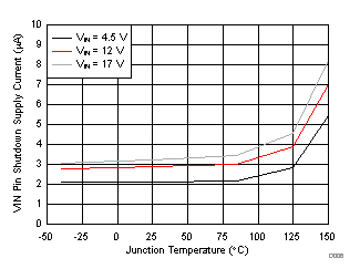
| V(EN) = 0.4 V |
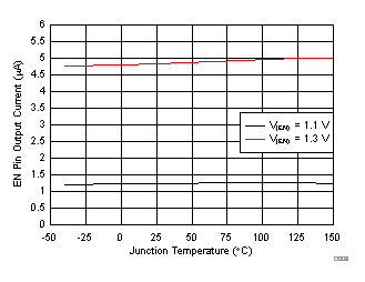
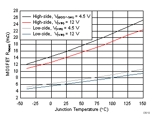
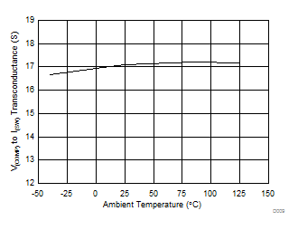
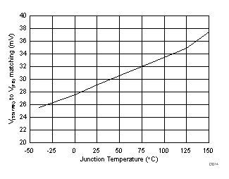
| V(SS/TRK) = 0.4 V |
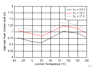
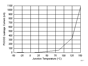
| V(FB) = 0.6 V | V(PGOOD) = 5 V |
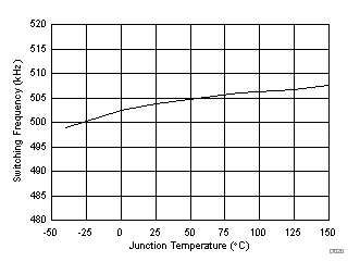
| R(RT/CLK) = 100 kΩ |
