ZHCSDR8 May   2015 TPS544B25 , TPS544C25

PRODUCTION DATA.  

  1. 特性
  2. 应用范围
  3. 说明
  4. 修订历史记录
  5. Device Comparison Table
  6. Pin Configuration and Functions
  7. Specifications
    1. 7.1 Absolute Maximum Ratings
    2. 7.2 ESD Ratings
    3. 7.3 Recommended Operating Conditions
    4. 7.4 Thermal Information
    5. 7.5 Electrical Characteristics
    6. 7.6 Typical Characteristics
  8. Detailed Description
    1. 8.1 Overview
    2. 8.2 Functional Block Diagram
    3. 8.3 Feature Description
      1. 8.3.1  Linear Regulators BP3 and BP6
      2. 8.3.2  Input Undervoltage Lockout (UVLO)
      3. 8.3.3  Turn-On and Turn-Off Delay and Sequencing
      4. 8.3.4  Voltage Reference
      5. 8.3.5  Differential Remote Sense
      6. 8.3.6  Set Output Voltage and Adapative Voltage Scaling (AVS)
        1. 8.3.6.1 Increasing the Output Voltage
        2. 8.3.6.2 Decreasing the Output Voltage
        3. 8.3.6.3 Set Default Output Voltage by VSET
      7. 8.3.7  Reset VOUT
      8. 8.3.8  Switching Frequency and Synchronization
      9. 8.3.9  Soft-Start and TON_RISE Command
      10. 8.3.10 Pre-Biased Output Start-Up
      11. 8.3.11 Soft-Stop and TOFF_FALL Command
      12. 8.3.12 Current Monitoring and Low-Side MOSFET Overcurrent Protection
      13. 8.3.13 High-Side MOSFET Short-Circuit Protection
      14. 8.3.14 Over-Temperature Protection
      15. 8.3.15 Output Overvoltage and Undervoltage Protection
      16. 8.3.16 TON_MAX Fault
      17. 8.3.17 Power Good (PGOOD) Indicator
      18. 8.3.18 Fault Protection Responses
      19. 8.3.19 Switching Node
      20. 8.3.20 PMBus General Description
      21. 8.3.21 PMBus Address
      22. 8.3.22 PMBus Connections
      23. 8.3.23 Auto ARA (Alert Response Address) Response
    4. 8.4 Device Functional Modes
      1. 8.4.1 Continuous Conduction Mode
      2. 8.4.2 Operation with CNTL Signal Control
      3. 8.4.3 Operation with OPERATION Control
      4. 8.4.4 Operation with CNTL and OPERATION Control
    5. 8.5 Supported PMBus Commands
    6. 8.6 Register Maps
      1. 8.6.1  OPERATION (01h)
        1. 8.6.1.1 On
        2. 8.6.1.2 Off
      2. 8.6.2  ON_OFF_CONFIG (02h)
        1. 8.6.2.1 pu
        2. 8.6.2.2 cmd
        3. 8.6.2.3 cpr
        4. 8.6.2.4 pol
        5. 8.6.2.5 cpa
      3. 8.6.3  CLEAR_FAULTS (03h)
      4. 8.6.4  WRITE_PROTECT (10h)
        1. 8.6.4.1 bit5
        2. 8.6.4.2 bit6
        3. 8.6.4.3 bit7
      5. 8.6.5  STORE_DEFAULT_ALL (11h)
      6. 8.6.6  RESTORE_DEFAULT_ALL (12h)
      7. 8.6.7  CAPABILITY (19h)
      8. 8.6.8  SMBALERT_MASK (1Bh)
      9. 8.6.9  VOUT_MODE (20h)
        1. 8.6.9.1 Mode:
        2. 8.6.9.2 Exponent
      10. 8.6.10 VOUT_COMMAND (21h)
        1. 8.6.10.1 Exponent
        2. 8.6.10.2 Mantissa
      11. 8.6.11 VOUT_MAX (24h)
        1. 8.6.11.1 Exponent
        2. 8.6.11.2 Mantissa
      12. 8.6.12 VOUT_TRANSITION_RATE (27h)
        1. 8.6.12.1 Exponent
        2. 8.6.12.2 Mantissa
      13. 8.6.13 VOUT_SCALE_LOOP (29h)
        1. 8.6.13.1 Exponent
        2. 8.6.13.2 Mantissa
      14. 8.6.14 VIN_ON (35h)
        1. 8.6.14.1 Exponent
        2. 8.6.14.2 Mantissa
      15. 8.6.15 VIN_OFF (36h)
        1. 8.6.15.1 Exponent
        2. 8.6.15.2 Mantissa
      16. 8.6.16 IOUT_CAL_OFFSET (39h)
        1. 8.6.16.1 Exponent
        2. 8.6.16.2 Mantissa
      17. 8.6.17 VOUT_OV_FAULT_LIMIT (40h)
        1. 8.6.17.1 Exponent
        2. 8.6.17.2 Mantissa
      18. 8.6.18 VOUT_OV_FAULT_RESPONSE (41h)
        1. 8.6.18.1 RSP[1]
        2. 8.6.18.2 RS[2:0]
      19. 8.6.19 VOUT_OV_WARN_LIMIT (42h)
        1. 8.6.19.1 Exponent
        2. 8.6.19.2 Mantissa
      20. 8.6.20 VOUT_UV_WARN_LIMIT (43h)
        1. 8.6.20.1 Exponent
        2. 8.6.20.2 Mantissa
      21. 8.6.21 VOUT_UV_FAULT_LIMIT (44h)
        1. 8.6.21.1 Exponent
        2. 8.6.21.2 Mantissa
      22. 8.6.22 VOUT_UV_FAULT_RESPONSE (45h)
        1. 8.6.22.1 RSP[1]
        2. 8.6.22.2 RS[2:0]
      23. 8.6.23 IOUT_OC_FAULT_LIMIT (46h)
        1. 8.6.23.1 Exponent
        2. 8.6.23.2 Mantissa
      24. 8.6.24 IOUT_OC_FAULT_RESPONSE (47h)
        1. 8.6.24.1 RSP[1]
        2. 8.6.24.2 RS[2:0]
      25. 8.6.25 IOUT_OC_WARN_LIMIT (4Ah)
        1. 8.6.25.1 Exponent
        2. 8.6.25.2 Mantissa
      26. 8.6.26 OT_FAULT_LIMIT (4Fh)
        1. 8.6.26.1 Exponent
        2. 8.6.26.2 Mantissa
      27. 8.6.27 OT_FAULT_RESPONSE (50h)
        1. 8.6.27.1 RSP[1]
        2. 8.6.27.2 RS[2:0]
      28. 8.6.28 OT_WARN_LIMIT (51h)
        1. 8.6.28.1 Exponent
        2. 8.6.28.2 Mantissa
      29. 8.6.29 TON_DELAY (60h)
        1. 8.6.29.1 Exponent
        2. 8.6.29.2 Mantissa
      30. 8.6.30 TON_RISE (61h)
        1. 8.6.30.1 Exponent
        2. 8.6.30.2 Mantissa
      31. 8.6.31 TON_MAX_FAULT_LIMIT (62h)
        1. 8.6.31.1 Exponent
        2. 8.6.31.2 Mantissa
      32. 8.6.32 TON_MAX_FAULT_RESPONSE (63h)
        1. 8.6.32.1 RSP[1]
        2. 8.6.32.2 RS[2:0]
      33. 8.6.33 TOFF_DELAY (64h)
        1. 8.6.33.1 Exponent
        2. 8.6.33.2 Mantissa
      34. 8.6.34 TOFF_FALL (65h)
        1. 8.6.34.1 Exponent
        2. 8.6.34.2 Mantissa
      35. 8.6.35 STATUS_BYTE (78h)
      36. 8.6.36 STATUS_WORD (79h)
      37. 8.6.37 STATUS_VOUT (7Ah)
      38. 8.6.38 STATUS_IOUT (7Bh)
      39. 8.6.39 STATUS_INPUT (7Ch)
      40. 8.6.40 STATUS_TEMPERATURE (7Dh)
      41. 8.6.41 STATUS_CML (7Eh)
      42. 8.6.42 STATUS_MFR_SPECIFIC (80h)
      43. 8.6.43 READ_VOUT (8Bh)
        1. 8.6.43.1 Exponent
        2. 8.6.43.2 Mantissa
      44. 8.6.44 READ_IOUT (8Ch)
        1. 8.6.44.1 Exponent
        2. 8.6.44.2 Mantissa
      45. 8.6.45 READ_TEMPERATURE_2 (8Eh)
        1. 8.6.45.1 Exponent
        2. 8.6.45.2 Mantissa
      46. 8.6.46 PMBUS_REVISION (98h)
      47. 8.6.47 MFR_VOUT_MIN (A4h)
        1. 8.6.47.1 Exponent
        2. 8.6.47.2 Mantissa
      48. 8.6.48 IC_DEVICE_ID (ADh)
      49. 8.6.49 IC_DEVICE_REV (AEh)
      50. 8.6.50 MFR_SPECIFIC_00 (D0h)
      51. 8.6.51 OPTIONS (MFR_SPECIFIC_21) (E5h)
        1. 8.6.51.1 PMB_HI_LO
        2. 8.6.51.2 PMB_VTH
        3. 8.6.51.3 EN_ADC_CNTL
        4. 8.6.51.4 VSM
        5. 8.6.51.5 DLO
        6. 8.6.51.6 AVG_PROG[1:0]
        7. 8.6.51.7 EN_AUTO_ARA
        8. 8.6.51.8 SS_DET_DIS
      52. 8.6.52 MISC_CONFIG_OPTIONS (MFR_SPECIFIC_32) (F0h)
        1. 8.6.52.1 OV_RESP_SEL
        2. 8.6.52.2 HSOC_USER_TRIM[1:0]
        3. 8.6.52.3 FORCE_SYNC
  9. Applications and Implementation
    1. 9.1 Application Information
    2. 9.2 Typical Applications
      1. 9.2.1 TPS544C25 4.5-V to 18-V Input, 0.95-V Output, 30-A Converter
      2. 9.2.2 Design Requirements
      3. 9.2.3 Design Procedure
        1. 9.2.3.1  Switching Frequency Selection
        2. 9.2.3.2  Inductor Selection
        3. 9.2.3.3  Output Capacitor Selection
          1. 9.2.3.3.1 Response to a Load Transient
          2. 9.2.3.3.2 Output Voltage Ripple
          3. 9.2.3.3.3 Bus Capacitance
        4. 9.2.3.4  Input Capacitor Selection
        5. 9.2.3.5  Bootstrap Capacitor Selection
        6. 9.2.3.6  BP6 and BP3
        7. 9.2.3.7  R-C Snubber and VIN Pin High-Frequency Bypass
        8. 9.2.3.8  Temperature Sensor
        9. 9.2.3.9  Key PMBus Parameter Selection
          1. 9.2.3.9.1 Enable, UVLO and Sequencing
          2. 9.2.3.9.2 Soft-Start Time
          3. 9.2.3.9.3 Overcurrent Threshold and Response
          4. 9.2.3.9.4 Power Good, Output Overvoltage and Undervoltage Protection
        10. 9.2.3.10 Output Voltage Setting and Frequency Compensation Selection
      4. 9.2.4 Application Curves
  10. 10Power Supply Recommendations
  11. 11Layout
    1. 11.1 Layout Guidelines
    2. 11.2 Layout Example
      1. 11.2.1 Mounting and Thermal Profile Recommendation
  12. 12器件和文档支持
    1. 12.1 器件支持
      1. 12.1.1 开发支持
        1. 12.1.1.1 米6体育平台手机版_好二三四 (TI) Fusion Digital Power Designer
        2. 12.1.1.2 TPS40k 环路补偿工具
    2. 12.2 相关链接
    3. 12.3 社区资源
    4. 12.4 商标
    5. 12.5 静电放电警告
    6. 12.6 Glossary
  13. 13机械、封装和可订购信息

封装选项

机械数据 (封装 | 引脚)
散热焊盘机械数据 (封装 | 引脚)
订购信息

Specifications

Absolute Maximum Ratings

over operating free-air temperature range (unless otherwise noted) (1)
MIN MAX UNIT
Input voltage range VIN, VDD –0.3 18 V
VIN, VDD <2 ms transient –0.3 19
VIN – SW (VIN to SW differential) –0.3 25
VIN – SW (VIN to SW differential, <10 ns transient due to SW ringing) –5 25
BOOT –0.3 37
BOOT – SW (BOOT to SW differential) –0.3 7
BOOT – SW (BOOT to SW differential, <10 ns transient) –0.3 7.5
CLK, DATA –0.3 5.5
VSET, ADDR0, ADDR1, TSNS/SS –0.3 3.6
FB, SYNC/RESET_B, CNTL, VOUTS–, VOUTS+, RT –0.3 7
Output voltage range SW –1 25 V
SW <100 ns transient –5 25
BP6, COMP, DIFFO, PGOOD –0.3 7
SMBALERT –0.3 5.5
BP3 –0.3 3.6
Operating junction temperature range, TJ –40 150 °C
Storage temperature range, Tstg –55 150
Stresses beyond those listed under Absolute Maximum Ratings may cause permanent damage to the device. These are stress ratings only, which do not imply functional operation of the device at these or any other conditions beyond those indicated under Recommended Operating Conditions. Exposure to absolute-maximum-rated conditions for extended periods may affect device reliability.

ESD Ratings

VALUE UNIT
V(ESD) Electrostatic discharge Human body model (HBM), per ANSI/ESDA/JEDEC JS-001, all pins(1) ±2000 V
Charged device model (CDM), per JEDEC specification JESD22-C101, all pins(2) ±1500
JEDEC document JEP155 states that 500-V HBM allows safe manufacturing with a standard ESD control process
JEDEC document JEP157 states that 250-V CDM allows safe manufacturing with a standard ESD control process.

Recommended Operating Conditions

over operating free-air temperature range (unless otherwise noted)
MIN TYP MAX UNIT
VDD Controller input voltage 4.5 12 18 V
VIN Power stage input voltage 4.5 12 18 V
TJ Junction temperature –40 125 °C

Thermal Information

THERMAL METRIC(1) TPS544x25 UNIT
PQFN (RVF)
40 PINS
RθJA Junction-to-ambient thermal resistance 27.4 °C/W
RθJC(top) Junction-to-case (top) thermal resistance 18.3
RθJB Junction-to-board thermal resistance 4.2
ψJT Junction-to-top characterization parameter 1.4
ψJB Junction-to-board characterization parameter 4.2
RθJC(bot) Junction-to-case (bottom) thermal resistance 1.0
For more information about traditional and new thermal metrics, see the IC Package Thermal Metrics application report, SPRA953.

Electrical Characteristics

TJ = –40°C to 125°C, VVIN = VVDD= 12 V, RRT = 40.2 kΩ; zero power dissipation (unless otherwise noted)
PARAMETER TEST CONDITIONS MIN TYP MAX UNIT
INPUT SUPPLY
VVDD Input supply voltage range 4.5 18 V
VVIN Power stage voltage range 4.5 18
IVDD Input operating current Not switching 9.5 12 mA
UVLO
VIN_ON Input turn on voltage Factory default setting 4.5 V
Programmable range, 15 different settings 4.25 7.75
Accuracy –5% 5%
VIN_OFF Input turn off voltage Factory default setting 4 V
Programmable range, 15 different settings 4 7.5
Accuracy –5% 5%
ERROR AMPLIFIER AND FEEDBACK VOLTAGE
VFB Feedback pin voltage Default setting 940.5 950 959.5 mV
Setpoint range(1) 0.5 1.5 V
VFB(ACC) Feedback pin voltage accuracy VFB = 600 mV, 0°C ≤ TJ ≤ 85°C(2) –0.5% 0.5% %
0.6 V ≤ VFB ≤ 1.5 V(1) –1.0% 1.0%
0.5 V ≤ VFB < 0.6 V(1) –1.5% 1.5%
AOL Open-loop gain(1) 80 dB
GBWP Gain bandwidth product(1) 15 MHz
IFB FB pin input bias current VFB = 0.95 V –75 75 nA
ICOMP Sourcing VFB = 0 V 1 mA
Sinking VFB = 1.2 V 1
VSET
IVset VSET pin current 9.5 10.5 12 µA
VVset Initial VOUT setting RVset = 34.8 kΩ 950 mV
VVset(dis) VSET disable threshold 2.41 V
OSCILLATOR
FSW Adjustment range(2) 200 1000 kHz
Switching frequency RRT = 40.2 kΩ 425 500 575 kHz
VRMP Ramp peak-to-peak(1) VVDD/9.3 VVDD/8.5 VVDD/7.6 V
VVLY Valley voltage(1) 0.75
SYNCHRONIZATION
VIH(sync) High-level input voltage 2.0 V
VIL(sync) Low-level input voltage 0.80
Tpw(sync) Sync input minimum pulse width 100 ns
fSYNC Synchronization frequency 200 1200 kHz
ΔfSYNC SYNC pin frequency range from free running frequency(1) -20% 20%
RESET_B
VIH(reset) High-level input voltage(1) 3.3-V and 5-V logic 2.1 V
1.8-V logic (factory default) 1.2
VIL(reset) Low-level input voltage 3.3-V and 5-V logic 0.8
1.8-V logic (factory default) 0.5
tPW(reset) Minimum RESET_B pulse width RVSET = 34.8 kΩ 200 ns
Vvout_command(reset) Output voltage after reset triggered RVSET = 34.8 kΩ 950 mV
BP6 REGULATOR
VBP6 Regulator output voltage IBP6 = 10 mA 5.85 6.4 6.9 V
VBP6(do) Regulator dropout voltage VVIN – VBP6, VVDD = 4.5 V, IBP6 = 25 mA 50 200 400 mV
IBP6SC Regulator short-circuit current(1) VVDD = 12 V 150 mA
VBP6UV Regulator UVLO voltage(1) 3.73 V
VBP6UV(hyst) Regulator UVLO voltage hysteresis(1) 320 mV
BOOTSTRAP
VBOOT(drop) Bootstrap voltage drop IBOOT = 5 mA 125 mV
BP3 REGULATOR
VBP3 3-V regulator output voltage VVDD ≥ 4.5 V, IBP3 = 5 mA 3.0 3.2 3.4 V
IBP3SC 3-V regulator short-circuit current(1) 35 mA
PWM
tON(min) Minimum controllable pulse width(1) 100 ns
SOFT-START
TON_RISE Soft-start time Factory default setting 5 ms
Programmable range, 16 discrete settings(1)(3) 0 100
Accuracy, TON_RISE = 1 ms -10 10 %
TON_MAX_FAULT_LIMIT Upper limit on the time to power up the output Factory default setting 100 ms
Programmable range, 16 discrete settings(1)(4) 0 100
Accuracy(1) –10 10 %
TON_DELAY Turn-on delay Factory default setting 0 ms
Programmable range, 16 discrete settings(1) 0 100
Accuracy(1) –10 10 %
SOFT-STOP
TOFF_FALL Soft-stop time Factory default setting(5) 0 ms
Programmable range, 16 discrete settings(1)(5) 0 100
Accuracy, TOFF_FALL = 1 ms –10 10 %
TOFF_DELAY Turn-off delay Factory default setting 0 ms
Programmable range, 16 discrete settings(1) 0 100
Accuracy(1) –10 10 %
SS PIN FOR INITIAL SOFT-START PROGRAMMING
ISS SS pin current 9.5 10.5 12 µA
VSS(ivlow) SS pin invalid low voltage 0.03 V
VSS(ivhigh) SS pin invalid high voltage 2.40
REMOTE SENSE AMPLIFIER
VDIFFO(err) Error voltage from DIFFO to (VOUTS+ – VOUTS–) (VOUTS+ – VOUTS–) = 0.6 V –5 5 mV
(VOUTS+ – VOUTS–) = 1.2 V –7 7
(VOUTS+ – VOUTS–) = 3.0 V –15 15
ARSA Differential gain 0.995 1.005 V/V
BWRSA Closed-loop bandwidth(1) 2 MHz
VDIFFO(max) Maximum DIFFO output voltage VBP6–0.2 V
IDIFFO DIFFO sourcing current 1 mA
DIFFO sinking current 1
POWER STAGE
RHS High-side power device on-resistance VVDD ≥ 12 V, TJ = 25°C 5.5
RLS Low-side power device on-resistance VVDD ≥ 12 V, (BOOT - SW) = 6.5 V, TJ = 25°C 2.0
CURRENT SENSE AMPLIFIER
tLS(minCS) Minimum LDRV pulse width for valid overcurrent and current mornitoring(1) 400 ns
LOW-SIDE CURRENT LIMIT PROTECTION
tOFF(OC) Off time between restart attempts(1) 7 × TON_RISE ms
IOUT_OC_FAULT_
LIMIT
Output current overcurrent fault threshold Factory default setting TPS544C25 36 A
Programmable range 5 40
Factory default setting TPS544B25 24
Programmable range 5 36
IOUT_OC_WARN_
LIMIT
Output current overcurrent warning threshold Factory default setting TPS544C25 34
Programmable range 4 39.5
Factory default setting TPS544B25 22
Programmable range 4 35.5
IOC(acc) Output current overcurrent fault accuracy IOUT ≥ 20 A –10% +10%
Output current overcurrent warning accuracy IOUT ≥ 20 A(1) –10% +10%
HIGH-SIDE SHORT CIRCUIT PROTECTION
IHSOC High-side short-circuit protection peak current threshold TPS544C25 40 75 A
TPS544B25 33 66
POWER GOOD (PGOOD) AND OVERVOLTAGE/UNDERVOLTAGE WARNING
VPG(hyst) PGOOD and over/under votlage warning threshold hysteresis at DIFFO pin VOUT_SCALE_LOOP = 1.0 15 75 mV
RPGOOD PGOOD pull-down resistance VDIFFO = 0 V, IPGOOD = 5 mA 30 45 60 Ω
IPGOOD(lk) PGOOD pin leakage current VPGOOD = 5 V 15 µA
VOUT_OV_WARN_LIMIT Overvoltage warning threshold at DIFFO pin VOUT_SCALE_LOOP = 1.0, factory default setting 1165 1201 1237 mV
VOUT_SCALE_LOOP = 1.0, programmable range(1) 527 1797
VOUT_UV_WARN_LIMIT Undervoltage warning threshold at DIFFO pin VOUT_SCALE_LOOP = 1.0, factory default setting 600 631 650
VOUT_SCALE_LOOP = 1.0, programmable range(1) 350 1428
VUVOV(warnhyst) Over/under votlage warning threshold hysteresis at DIFFO pin VOUT_SCALE_LOOP = 1.0(1) 15 75
OUTPUT OVERVOLTAGE AND UNDERVOLTAGE FAULT PROTECTION
VOUT_OV_FAULT_LIMIT Overvoltage fault threshold at DIFFO pin VOUT_SCALE_LOOP = 1.0, factory default setting 1243 1281 1330 mV
VOUT_SCALE_LOOP = 1.0, programmable range(1) 529 1799
VOUT_UV_FAULT_LIMIT Undervoltage fault threshold at DIFFO pin VOUT_SCALE_LOOP = 1.0, factory default setting 550 594 610
VOUT_SCALE_LOOP = 1.0, programmable range(1)(4) 346 1426
VUVOV(flthyst) Over/under votlage fault threshold hysteresis at DIFFO pin VOUT_SCALE_LOOP = 1.0(1) 15 75
OUTPUT VOLTAGE TRIMMING
VOUT_
TRANSITION_
RATE
Output voltage transition rate Factory default setting 1.0 mV/µs
Programmable range, 8 discrete settings 0.067 1.5
Accuracy –10% 10%
VOUT_SCALE_
LOOP
Feedback loop scaling factor Factory default setting 1
Programmable range, 3 discrete settings 0.25 1
VOUT_COMMAND Output voltage programmable register value, multiply by 2-9 to get output voltage Factor default setting 486
VOUT_SCALE_LOOP = 1.0, programmable range(1) 256 768
VOUT_SCALE_LOOP = 0.5, programmable range(1) 512 1536
VOUT_SCALE_LOOP = 0.25, programmable range(1) 1024 3072
TEMPERATURE SENSE AND THERMAL SHUTDOWN
TSD Junction thermal shutdown temperature(1) 135 145 155 °C
THYST Junction thermal shutdown hysteresis(1) 15 20 25
VTSNS Voltage range on TSNS/SS pin(1) 0 1.00 V
OT_FAULT_LIMIT External overtemperature fault limit(1) Factory default setting 125 °C
Programmable range 120 165
OT_WARN_LIMIT External overtemperature warning limit(1) Factory default setting 100
Programmable range 100 140
TOT(hys) External overtemperature fault, warning hysteresis(1) 15 20 25
MEASUREMENT SYSTEM
MVOUT(rng) Output voltage measurement range 0.5 5.8 V
MVOUT(acc) Output voltage measurement accuracy –2.0% 2.0%
MVOUT(lsb) Output voltage measurement bit resolution(1) 1.953 mV
MIOUT(rng) Output current measurement range 0 40 A
MIOUT(acc) Output current measurement accuracy IOUT ≥ 20 A –15% 15%
3 A ≤ IOUT < 20 A(1) –3 3 A
MIOUT(lsb) Output current measurement bit resolution(1) 62.5 mA
MTSNS(rng) External temperature sense range(1) –40 165 °C
MTSNS(acc) External temperature sense accuracy(1) -40°C ≤ TJ(sensor) ≤ 165°C –5 5
MTSNS(lsb) External temperature sense bit resolution(1) 1
PMBus INTERFACE ADDRESSING
IADD Address pin bias current 9.5 10.5 12 µA
VADD(ivlow) Address pin illegal low voltage 0.05 V
VADD(ivhigh) Address pin illegal high voltage 2.40
PMBus™ INTERFACE
VIH Input high voltage, CLK, DATA, CNTL 3.3-V/5-V logic 2.1 V
1.8-V logic (factory default) 1.2
VIL Input low voltage, CLK, DATA, CNTL 3.3-V/5-V logic 0.8 V
1.8-V logic (factory default) 0.5
IIH Input high level current, CLK, DATA -10 10 µA
IIL Input low level current, CLK, DATA -10 10 µA
ICNTL CNTL pin pull-up current 5 10 µA
VOL Output low level voltage, DATA, SMBALERT VDD > 4.5 V, input current to DATA, SMBALERT = 4mA 0.4 V
IOH Output high level open drain leakage current, DATA, SMBALERT Voltage on DATA, SMBALERT = 5.5V -10 10 µA
IOL Output low level open drain leakage current, DATA, SMBALERT Voltage on DATA, SMBALERT = 0.4V 4.0 mA
IPMB PMBus operating frequency range Slave mode 10 400 kHz
Specified by design. Not production tested.
The parameter covers 4.5 V to 18 V of VDD.
The setting of TON_RISE of 0 ms means the unit to bring its output voltage to the programmed regulation value as quickly as possible, which results in an effective TON_RISE time of 1 ms (fastest time supported).
The setting of TON_MAX_FAULT_LIMIT and VOUT_UV_FAULT_LIMIT of 0 means disabling TON_MAX_FAULT and VOUT_UV_FAULT response and reporting, respectively.
The setting of TOFF_FALL of 0 ms means the unit to bring its output voltage down to 0 as quickly as possible, which results in an effective TOFF_FALL time of 1 ms (fastest time supported).

Typical Characteristics

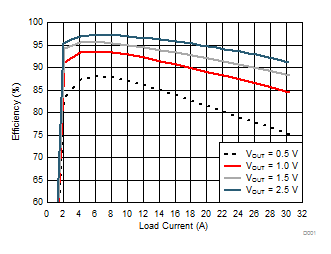
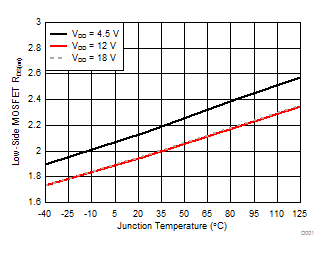
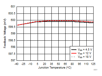
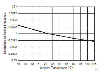
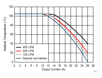
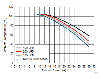
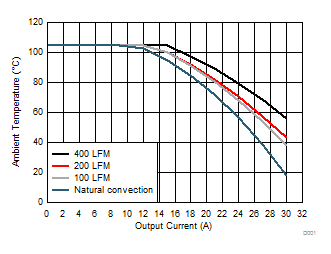
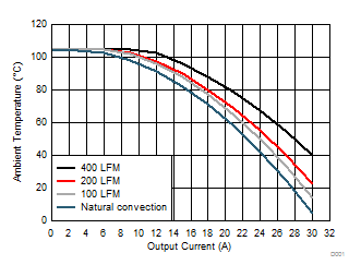
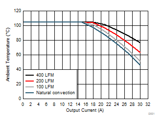
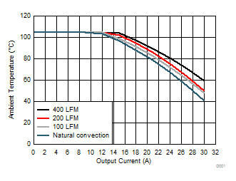
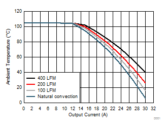
VIN = VDD = 12 V, TA = 25 ºC, RRT = 40.2 kΩ (unless otherwise specified). Safe operating area curves were measured using a Texas Instruments Evaluation Module.
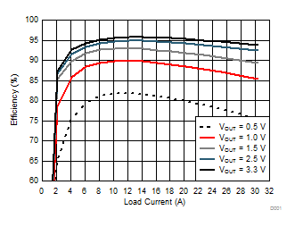
TPS544C25 TPS544B25 D001_SLUSC81.gif
VIN = 5 V L = 470 nH No Snubber
fSW = 500 kHz RDCR = 0.3 mΩ RBOOT = 0 Ω
Figure 1. Efficiency vs. Output Current
TPS544C25 TPS544B25 D016_SLUSC81.gif
Figure 3. Low-Side MOSFET On-Resistance (RDS(on))
vs. Junction Temperature
TPS544C25 TPS544B25 D018_SLUSC81.gif
VFB = 600 mV
Figure 5. Feedback Voltage vs. Junction Temperature
TPS544C25 TPS544B25 D025_SLUSC81.gif
Figure 7. Normalized Switching Frequency
vs. Junction Temperature
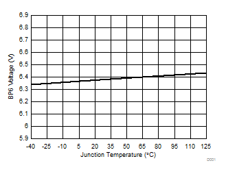
TPS544C25 TPS544B25 D023_SLUSC81.gif
IBP6 = 10 mA VVIN = VVDD= 12 V
Figure 9. BP6 Voltage vs. Junction Temperature
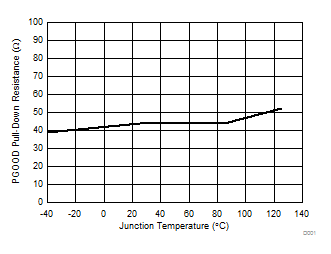
TPS544C25 TPS544B25 D026_SLUSC81.gif
Figure 11. PGOOD Pull-Down Resistance
vs. Junction Temperature
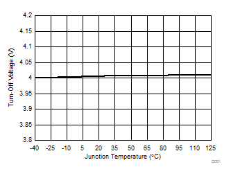
TPS544C25 TPS544B25 D022_SLUSC81.gif
VIN_OFF = 4.0 V
Figure 13. Turn-Off Voltage vs. Junction Temperature
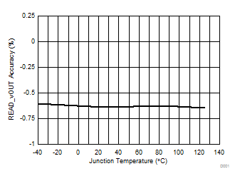
TPS544C25 TPS544B25 D028_SLUSC81.gif
VVIN = VVDD= 12 V
Figure 15. READ_VOUT Accuracy vs. Junction Temperature
TPS544C25 TPS544B25 D030_SLUSC81.gif
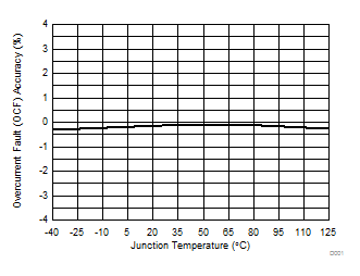
OCF = 20 A VVIN = VVDD= 12 V
Figure 17. Overcurrent Fault Protection (OCF) Accuracy
vs. Junction Temperature
TPS544C25 TPS544B25 D003_SLUSC81.gif
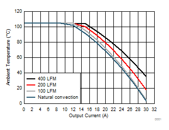
VIN = 5 V VOUT = 1.0 V fSW = 1 MHz
Figure 19. Safe Operating Area
TPS544C25 TPS544B25 D005_SLUSC81.gif
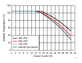
VIN = 5 V VOUT = 1.0 V fSW = 500 kHz
Figure 21. Safe Operating Area
TPS544C25 TPS544B25 D015_SLUSC81.gif
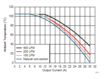
VIN = 5 V VOUT = 1.5 V fSW = 500 kHz
Figure 23. Safe Operating Area
TPS544C25 TPS544B25 D008_SLUSC81.gif
VIN = 5 V VOUT = 3.3 V fSW = 500 kHz
Figure 25. Safe Operating Area
TPS544C25 TPS544B25 D010_SLUSC81.gif
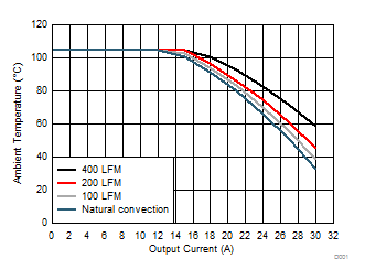
VIN = 12 V VOUT = 1.0 V fSW = 500 kHz
Figure 27. Safe Operating Area
TPS544C25 TPS544B25 D012_SLUSC81.gif
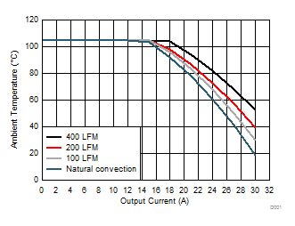
VIN = 12 V VOUT = 1.5 V fSW = 500 kHz
Figure 29. Safe Operating Area
TPS544C25 TPS544B25 D014_SLUSC81.gif
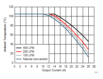
VIN = 12 V VOUT = 3.3 V fSW = 500 kHz
Figure 31. Safe Operating Area
TPS544C25 TPS544B25 D002_SLUSC81.gif
VIN = 12 V L = 470 nH No Snubber
fSW = 500 kHz RDCR = 0.3 mΩ RBOOT = 0 Ω
Figure 2. Efficiency vs. Output Current
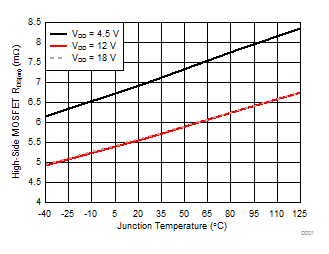
TPS544C25 TPS544B25 D017_SLUSC81.gif
Figure 4. High-Side MOSFET On-Resistance (RDS(on))
vs. Junction Temperature
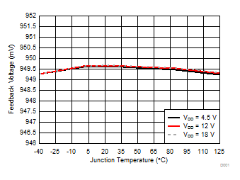
TPS544C25 TPS544B25 D019_SLUSC81.gif
VFB = 950 mV
Figure 6. Feedback Voltage vs. Junction Temperature
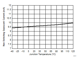
TPS544C25 TPS544B25 D020_SLUSC81.gif
Figure 8. Non-Switching Input Current (IVDD)
vs. Junction Temperature
TPS544C25 TPS544B25 D024_SLUSC81.gif
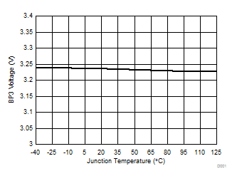
IBP3 = 5 mA VVIN = VVDD= 12 V
Figure 10. BP3 Voltage vs. Junction Temperature
TPS544C25 TPS544B25 D021_SLUSC81.gif
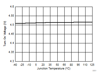
VIN_ON = 4.5 V
Figure 12. Turn-On Voltage vs. Junction Temperature
TPS544C25 TPS544B25 D027_SLUSC81.gif
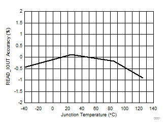
IOUT = 20 A VVIN = VVDD= 12 V
Figure 14. READ_IOUT Accuracy vs. Junction Temperature
TPS544C25 TPS544B25 D029_SLUSC81.gif
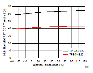
BOOT - SW = 6.5 V VVIN = VVDD= 12 V
Figure 16. High-Side Overcurrent Protection
vs. Junction Temperature
TPS544C25 TPS544B25 D031_SLUSC81.gif
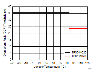
VVIN = VVDD= 12 V OCF = 36 A (TPS544C25) OCF = 24 A (TPS544B25)
Figure 18. Overcurrent Fault Protection (OCF)
vs. Junction Temperature
TPS544C25 TPS544B25 D004_SLUSC81.gif
VIN = 5 V VOUT = 1.0 V fSW = 300 kHz
Figure 20. Safe Operating Area
TPS544C25 TPS544B25 D006_SLUSC81.gif
VIN = 5 V VOUT = 1.5 V fSW = 300 kHz
Figure 22. Safe Operating Area
TPS544C25 TPS544B25 D007_SLUSC81.gif
VIN = 5 V VOUT = 3.3 V fSW = 300 kHz
Figure 24. Safe Operating Area
TPS544C25 TPS544B25 D009_SLUSC81.gif
VIN = 12 V VOUT = 1.0 V fSW = 300 kHz
Figure 26. Safe Operating Area
TPS544C25 TPS544B25 D011_SLUSC81.gif
VIN = 12 V VOUT = 1.5 V fSW = 300 kHz
Figure 28. Safe Operating Area
TPS544C25 TPS544B25 D013_SLUSC81.gif
VIN = 12 V VOUT = 3.3 V fSW = 300 kHz
Figure 30. Safe Operating Area