ZHCSDR8 May 2015 TPS544B25 , TPS544C25
PRODUCTION DATA.
- 1 特性
- 2 应用范围
- 3 说明
- 4 修订历史记录
- 5 Device Comparison Table
- 6 Pin Configuration and Functions
- 7 Specifications
-
8 Detailed Description
- 8.1 Overview
- 8.2 Functional Block Diagram
- 8.3
Feature Description
- 8.3.1 Linear Regulators BP3 and BP6
- 8.3.2 Input Undervoltage Lockout (UVLO)
- 8.3.3 Turn-On and Turn-Off Delay and Sequencing
- 8.3.4 Voltage Reference
- 8.3.5 Differential Remote Sense
- 8.3.6 Set Output Voltage and Adapative Voltage Scaling (AVS)
- 8.3.7 Reset VOUT
- 8.3.8 Switching Frequency and Synchronization
- 8.3.9 Soft-Start and TON_RISE Command
- 8.3.10 Pre-Biased Output Start-Up
- 8.3.11 Soft-Stop and TOFF_FALL Command
- 8.3.12 Current Monitoring and Low-Side MOSFET Overcurrent Protection
- 8.3.13 High-Side MOSFET Short-Circuit Protection
- 8.3.14 Over-Temperature Protection
- 8.3.15 Output Overvoltage and Undervoltage Protection
- 8.3.16 TON_MAX Fault
- 8.3.17 Power Good (PGOOD) Indicator
- 8.3.18 Fault Protection Responses
- 8.3.19 Switching Node
- 8.3.20 PMBus General Description
- 8.3.21 PMBus Address
- 8.3.22 PMBus Connections
- 8.3.23 Auto ARA (Alert Response Address) Response
- 8.4 Device Functional Modes
- 8.5 Supported PMBus Commands
- 8.6
Register Maps
- 8.6.1 OPERATION (01h)
- 8.6.2 ON_OFF_CONFIG (02h)
- 8.6.3 CLEAR_FAULTS (03h)
- 8.6.4 WRITE_PROTECT (10h)
- 8.6.5 STORE_DEFAULT_ALL (11h)
- 8.6.6 RESTORE_DEFAULT_ALL (12h)
- 8.6.7 CAPABILITY (19h)
- 8.6.8 SMBALERT_MASK (1Bh)
- 8.6.9 VOUT_MODE (20h)
- 8.6.10 VOUT_COMMAND (21h)
- 8.6.11 VOUT_MAX (24h)
- 8.6.12 VOUT_TRANSITION_RATE (27h)
- 8.6.13 VOUT_SCALE_LOOP (29h)
- 8.6.14 VIN_ON (35h)
- 8.6.15 VIN_OFF (36h)
- 8.6.16 IOUT_CAL_OFFSET (39h)
- 8.6.17 VOUT_OV_FAULT_LIMIT (40h)
- 8.6.18 VOUT_OV_FAULT_RESPONSE (41h)
- 8.6.19 VOUT_OV_WARN_LIMIT (42h)
- 8.6.20 VOUT_UV_WARN_LIMIT (43h)
- 8.6.21 VOUT_UV_FAULT_LIMIT (44h)
- 8.6.22 VOUT_UV_FAULT_RESPONSE (45h)
- 8.6.23 IOUT_OC_FAULT_LIMIT (46h)
- 8.6.24 IOUT_OC_FAULT_RESPONSE (47h)
- 8.6.25 IOUT_OC_WARN_LIMIT (4Ah)
- 8.6.26 OT_FAULT_LIMIT (4Fh)
- 8.6.27 OT_FAULT_RESPONSE (50h)
- 8.6.28 OT_WARN_LIMIT (51h)
- 8.6.29 TON_DELAY (60h)
- 8.6.30 TON_RISE (61h)
- 8.6.31 TON_MAX_FAULT_LIMIT (62h)
- 8.6.32 TON_MAX_FAULT_RESPONSE (63h)
- 8.6.33 TOFF_DELAY (64h)
- 8.6.34 TOFF_FALL (65h)
- 8.6.35 STATUS_BYTE (78h)
- 8.6.36 STATUS_WORD (79h)
- 8.6.37 STATUS_VOUT (7Ah)
- 8.6.38 STATUS_IOUT (7Bh)
- 8.6.39 STATUS_INPUT (7Ch)
- 8.6.40 STATUS_TEMPERATURE (7Dh)
- 8.6.41 STATUS_CML (7Eh)
- 8.6.42 STATUS_MFR_SPECIFIC (80h)
- 8.6.43 READ_VOUT (8Bh)
- 8.6.44 READ_IOUT (8Ch)
- 8.6.45 READ_TEMPERATURE_2 (8Eh)
- 8.6.46 PMBUS_REVISION (98h)
- 8.6.47 MFR_VOUT_MIN (A4h)
- 8.6.48 IC_DEVICE_ID (ADh)
- 8.6.49 IC_DEVICE_REV (AEh)
- 8.6.50 MFR_SPECIFIC_00 (D0h)
- 8.6.51 OPTIONS (MFR_SPECIFIC_21) (E5h)
- 8.6.52 MISC_CONFIG_OPTIONS (MFR_SPECIFIC_32) (F0h)
-
9 Applications and Implementation
- 9.1 Application Information
- 9.2
Typical Applications
- 9.2.1 TPS544C25 4.5-V to 18-V Input, 0.95-V Output, 30-A Converter
- 9.2.2 Design Requirements
- 9.2.3
Design Procedure
- 9.2.3.1 Switching Frequency Selection
- 9.2.3.2 Inductor Selection
- 9.2.3.3 Output Capacitor Selection
- 9.2.3.4 Input Capacitor Selection
- 9.2.3.5 Bootstrap Capacitor Selection
- 9.2.3.6 BP6 and BP3
- 9.2.3.7 R-C Snubber and VIN Pin High-Frequency Bypass
- 9.2.3.8 Temperature Sensor
- 9.2.3.9 Key PMBus Parameter Selection
- 9.2.3.10 Output Voltage Setting and Frequency Compensation Selection
- 9.2.4 Application Curves
- 10Power Supply Recommendations
- 11Layout
- 12器件和文档支持
- 13机械、封装和可订购信息
9 Applications and Implementation
9.1 Application Information
The TPS544x25 devices are highly-integrated synchronous step-down DC-DC converters. These devices are used to convert a higher DC input voltage to a lower DC output voltage, with a maximum output current of 20 A or 30 A. Use the following design procedure to select key component values for this family of devices, and set the appropriate behavioral options via the PMBus™ interface.
9.2 Typical Applications
9.2.1 TPS544C25 4.5-V to 18-V Input, 0.95-V Output, 30-A Converter
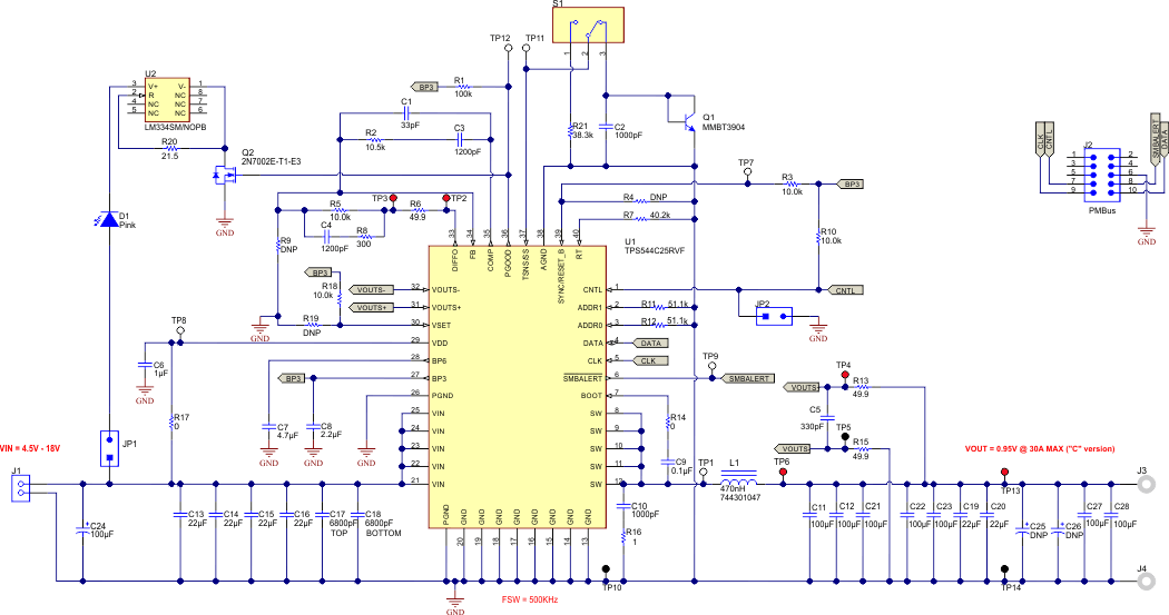 Figure 44. Typical Application Schematic
9.2.2 Design Requirements
For this design example, use the following input parameters.
Table 16. Design Example Specifications
| PARAMETER | TEST CONDITION | MIN | TYP | MAX | UNIT | |
|---|---|---|---|---|---|---|
| VIN | Input voltage | 4.5 | 12.0 | 18.0 | V | |
| VIN(ripple) | Input ripple voltage | IOUT = 30 A | 0.4 | V | ||
| VOUT | Output voltage | 0.95 | V | |||
| Line regulation | 4.5 V ≤ VIN ≤ 18 V | 0.5% | ||||
| Load regulation | 0 V ≤ IOUT ≤ 30 A | 0.5% | ||||
| VPP | Output ripple voltage | IOUT = 30 A | 20 | mV | ||
| VOVER | Transient response overshoot | ISTEP = 10 A | 90 | mV | ||
| VUNDER | Transient response undershoot | ISTEP = 10 A | 90 | mV | ||
| IOUT | Output current | 4.5 V ≤ VIN ≤ 18 V | 0 | 20 | 30 | A |
| tSS | Soft-start time | VIN = 12 V | 5 | ms | ||
| IOC | Overcurrent trip point | 36 | 40 | A | ||
| η | Peak Efficiency | IOUT = 13 A, VIN = 12 V | 88% | |||
| fSW | Switching frequency | 500 | kHz | |||
9.2.3 Design Procedure
9.2.3.1 Switching Frequency Selection
Select a switching frequency for the regulator. There is a trade off between higher and lower switching frequencies. Higher switching frequencies may produce smaller a solution size using lower valued inductors and smaller output capacitors compared to a power supply that switches at a lower frequency. However, the higher switching frequency causes extra switching losses, which decrease efficiency and impact thermal performance. In this design, a moderate switching frequency of 500 kHz achieves both a small solution size and a high-efficiency operation With the frequency selected, the timing resistor is calculated using Equation 11

9.2.3.2 Inductor Selection
To calculate the value of the output inductor, use Equation 12. The coefficient KIND represents the amount of inductor ripple current relative to the maximum output current. The output capacitor filters the inductor ripple current. Therefore, choosing a high inductor ripple current impacts the selection of the output capacitor since the output capacitor must have a ripple current rating equal to or greater than the inductor ripple current. Generally, KIND coefficient should be kept between 0.2 and 0.4 for balanced performance. Using this target ripple current, the required inductor size can be calculated as shown in Equation 12

Selecting KIND = 0.3, the target inductance L1 = 200 nH. Using the next standard value, the 470 nH is chosen in this application for its high current rating, low DCR, and small size. The inductor ripple current, RMS current, and peak current can be calculated using Equation 13, Equation 14 and Equation 15. These values should be used to select an inductor with approximately the target inductance value, and current ratings that allow normal operation with some margin.


The Pulse PG077.401NL is rated for 45 ARMS current, and 48-A saturation. Using this inductor, the ripple current IRIPPLE= 3.85 A, the RMS inductor current IL(rms)= 30.02 A, and peak inductor current IL(peak)= 31.92 A.
9.2.3.3 Output Capacitor Selection
There are three primary considerations for selecting the value of the output capacitor. The output capacitor affects three criteria:
- how the regulator responds to a change in load current or load transient
- the output voltage ripple
- the amount of capacitance on the output voltage bus
The last of these three considerations is important when designing regulators that must operate where the electrical conditions are unpredictable. The output capacitance needs to be selected based on the most stringent of these three criteria.
9.2.3.3.1 Response to a Load Transient
The desired response to a load transient is the first criterion. The output capacitor needs to supply the load with the required current when not immediately provided by the regulator. When the output capacitor supplies load current, the impedance of the capacitor greatly affects the magnitude of voltage deviation during the transient.
In order to meet the requirements for control loop stability, the TPS544C25 requires the addition of compensation components in the design of the error amplifier. While these compensation components provide for a stable control loop, they often also reduce the speed with which the regulator can respond to load transients. The delay in the regulator response to load changes can be two or more clock cycles before the control loop reacts to the change. During that time the difference between the old and the new load current must be supplied (or absorbed) by the output capacitance. The output capacitor impedance must be designed to be able to supply or absorb the delta current while maintaining the output voltage within acceptable limits. Equation 16 and Equation 17 show the relationship between the transient response overshoot, VOVER, the transient response undershoot, VUNDER, and the required output capacitance, COUT.


where
- VIN(min) > 2 × VOUT, use overshoot to calculate minimum output capacitance.
- VIN(min) < 2 × VOUT, use undershoot to calculate minimum output capacitance.
In this case, the minimum designed input voltage VIN(min) is greater than 2 × VOUT, so VOVER dictates the minimum output capacitance. Therefore, using Equation 18, the minimum output capacitance required to meet the transient requirement is 285 µF.

9.2.3.3.2 Output Voltage Ripple
The output voltage ripple is the second criterion. Equation 19 calculates the minimum output capacitance required to meet the output voltage ripple specification. This criterion is the requirement when the impedance of the output capacitance is dominated by ESR.

In this case, the maximum output voltage ripple is 20 mV. Under this requirement, the minimum output capacitance for ripple (as calculated in Equation 19) yields 48 μF. Because this capacitance value is smaller than the output capacitance required to meet the transient response, select the output capacitance value based on the transient requirement. For this application, seven 100-µF low-ESR ceramic capacitors, and two 22-µF ceramic capacitors were selected to meet the transient specification with sufficient margin. Therefore COUT = 744 µF.
With the target output capacitance value chosen, Equation 20 calculates the maximum ESR the output capacitor bank can have to meet the output voltage ripple specification. Equation 20 indicates the ESR should be less than 4.9 mΩ. The ceramic capacitors each contribute approximately 3 mΩ, making the effective ESR of the output capacitor bank approximately 0.3 mΩ, meeting the specification with sufficient margin.

Additional capacitance de-ratings for aging, temperature and DC bias should be factored in, which increases the minimum required capacitance value. Capacitors generally have limits to the amount of ripple current they can handle without failing or producing excess heat. An output capacitor that can support the inductor ripple current must be specified. Some capacitor data sheets specify the RMS (root mean square) value of the maximum ripple current. Equation 21 can be used to calculate the RMS ripple current the output capacitor needs to support. For this application, Equation 21 yields 1.11 A.

9.2.3.3.3 Bus Capacitance
The amount of bus capacitance is the third criterion. This requirement is optional. However, extra output bus capacitance should be considered in systems where the electrical environment is unpredictable, or not fully defined, or can be subject to severe events such as hot-plug events or even electrostatic discharge (ESD) events.
During a hot-plug event, when a discharged load capacitor is plugged into the output of the regulator, the instantaneous current demand required to charge this load capacitance is be far too rapid to be supplied by the control loop. Often the peak charging current can be multiple times higher than the current limit of the regulator. Additional output capacitance helps maintain the bus voltage within acceptable limits. For hot-plug events, the amount of required bus capacitance can be calculated if the load capacitance is known, based on the concept of conservation of charge.
An ESD event, or even non-direct lightning surges at the primary circuit level can cause glitches at this converter system level. A glitch of sufficient amplitude to falsely trip OVP or UVLO can cause several clock cycles of disturbance. In such cases it is beneficial to design in more bus capacitance than is required by the simpler load transient and ripple requirements. The amount of extra bus capacitance can be calculated based on maintaining the output voltage within acceptable limits during the disturbance. This capacitance can be as much as required to fully support the load for the duration of the interrupted converter operation.
9.2.3.4 Input Capacitor Selection
The TPS544x25 devices require a high-quality, ceramic, type X5R or X7R, input decoupling capacitor with a value of at least 0.1 μF of effective capacitance on the VDD pin, relative to AGND. The power stage input decoupling capacitance (effective capacitance at the VIN and GND pins) must be sufficient to supply the high switching currents demanded when the high-side MOSFET switches on, while providing minimal input voltage ripple as a result. This effective capacitance includes any DC bias effects. The voltage rating of the input capacitor must be greater than the maximum input voltage. The capacitor must also have a ripple current rating greater than the maximum input current ripple to the device during full load. The input ripple current can be calculated using Equation 22.

The minimum input capacitance and ESR values for a given input voltage ripple specification, VIN(ripple), are shown in Equation 23 and Equation 24. The input ripple is composed of a capacitive portion, VRIPPLE(cap), and a resistive portion, VRIPPLE(esr).


The value of a ceramic capacitor varies significantly over temperature and the amount of DC bias applied to the capacitor. The capacitance variations due to temperature can be minimized by selecting a dielectric material that is stable over temperature. X5R and X7R ceramic dielectrics are usually selected for power regulator capacitors because they have a high capacitance to volume ratio and are fairly stable over temperature. The input capacitor must also be selected with the DC bias taken into account. For this example design, a ceramic capacitor with at least a 25-V voltage rating is required to support the maximum input voltage. For this design, allow 0.1-V input ripple for VRIPPLE(cap), and 0.3-V input ripple for VRIPPLE(esr). Using Equation 23 and Equation 24, the minimum input capacitance for this design is 32 µF, and the maximum ESR is 9.4 mΩ. For this example, four 22-μF, 25-V ceramic capacitors and one additional 100-μF, 25-V low-ESR polymer capacitors in parallel were selected for the power stage. For the VDD pin, one 1-μF, 25-V ceramic capacitor was selected. The input voltage (VDD) and power input voltage (VIN) pins must be tied together.
9.2.3.5 Bootstrap Capacitor Selection
A ceramic capacitor with a value of 0.1 μF must be connected between the BOOT and SW pins for proper operation. It is recommended to use a ceramic capacitor with X5R or better grade dielectric. The capacitor should have voltage rating of 25 V or higher.
9.2.3.6 BP6 and BP3
According to the recommendations in , BP3 is bypassed to AGND with 2.2 μF of capacitance, and BP6 is bypassed to PGND with 4.7-µF of capacitance. In order for the regulator to function properly, it is important that these capacitors be localized to the TPS544x25 , with low-impedance return paths. See for more information.
9.2.3.7 R-C Snubber and VIN Pin High-Frequency Bypass
Though it is possible to operate the TPS544x25 within absolute maximum ratings without ringing reduction techniques, some designs may require external components to further reduce ringing levels. This example uses two approaches: a high frequency power stage bypass capacitor on the VIN pins, and an R-C snubber between the SW area and GND.
The high-frequency VIN bypass capacitor is a lossless ringing reduction technique which helps minimizes the outboard parasitic inductances in the power stage, which store energy during the low-side MOSFET on-time, and discharge once the high-side MOSFET is turned on. For this example two 6.8-nF, 25-V, 0402 sized high-frequency capacitors are used. The placement of these capacitors is critical to its effectiveness. Its ideal placement is shown in .
Additionally, an R-C snubber circuit is added to this example. To balance efficiency and spike levels, a 1-nF capacitor and a 1-Ω resistor are chosen. In this example a 1206 resistor is chosen, which is rated for 0.25 W, nearly twice the estimated power dissipation. See SLUP100 for more information about snubber circuits.
9.2.3.8 Temperature Sensor
This application design uses a surface-mount MMBT3904 for the temperature sensor, Q1. In this example, the sensor monitors the PCB temperature where it is generally the highest, next to the power inductor. Placement of the temperature sensor and routing back to the TSNS pin are critical design features to reduce noise its temperature measurements. In this example, the temperature sensor is placed on the VOUT side of the power inductor to avoid switching noise from the SW plane, and routed back to the TSNS and AGND pin. Additionally, a 1-nF capacitor, C2, is placed from TSNS to AGND near the TSNS pin. The READ_TEMPERATURE_2 (8Eh) register is continually updated with the digitized temperature measurement, enabling temperature telemetry.
Disable external temperature sensing by terminating TSNS to AGND with a 0 Ω resistor. This termination forces the temperature readings to –40 °C, and prevents external over-temperature fault trips.
The switch S1 in this example can be used to switch between temperature sensor and SS resistor. Note that the READ_TEMPERATURE_2 value will be kept at 25°C when SS_DET_DIS in (E5h) MFR_SPECIFIC_21 is set to 0 since the TSNS/SS pin is configured to set TON_RISE time and not used for external temperature sensing.
9.2.3.9 Key PMBus™ Parameter Selection
Several of the key design parameters for the TPS544x25 device can be configured via the PMBus interface, and stored to its non-volatile memory (NVM) for future use.
9.2.3.9.1 Enable, UVLO and Sequencing
The ON_OFF_CONFIG (02h) command is used to select the turn-on behavior of the converter. For this example, the CNTL pin was used to enable or disable the converter, regardless of the state of OPERATION (01h), as long as input voltage is present, and above the UVLO threshold.
The minimum input voltage, VIN(min) , for this example is 4.5 V. The VIN_ON command was set to 4.5 V, and the VIN_OFF command was set to 4.0 V, giving 500 mV of hysteresis. If VIN falls below VIN_OFF, power conversion stops, until it is raised above VIN_ON.
The turn-on or turn-off delay time can be set by TON_DELAY and TOFF_DELAY. Accounting for the time during which the COMP signal rises to the valley of the PWM ramp, the delay between enabling power conversion, and the rise of the output voltage is approximately 200 µs. See Soft-Start and TON_RISE Command for more information.
9.2.3.9.2 Soft-Start Time
The TON_RISE command sets the soft-start time. When selecting the soft-start time, consider the charging current for the output capacitors. In some applications (e.g., those with large amounts of output capacitance) this current can lead to problems with nuisance tripping of the overcurrent protection circuitry. To avoid nuisance tripping, the output capacitor charging current should be included when choosing a soft-start time, and overcurrent threshold. The capacitor charging current can be calculated using Equation 25

With the charging current calculated, the overcurrent threshold can then be calibrated to the sum of the maximum load current and the output capacitor charging current plus some margin.
In this example, the soft-start time is arbitrarily selected to be 5 ms. In this case, the charging current, ICAP = 141.36 mA.
9.2.3.9.3 Overcurrent Threshold and Response
The IOUT_OC_FAULT_LIMIT command sets the overcurrent threshold. The current limit should be set to the maximum load current, plus the output capacitor charging current during start-up, plus some margin for load transients and component variation. The amount of margin required depends on the individual application, but a suggested starting point is between 25% and 30%. More or less may be required. For this application, the maximum load current is 30 A, the output capacitor charging current is 141 mA. This design allows some extra margin, so an overcurrent threshold of 36 A was selected.
The IOUT_OC_FAULT_RESPONSE command sets the desired response to an overcurrent event, which can be hiccup (continuously restart waiting for a 7 x soft-start time-out between re-trials) in the event of an overcurrent, latch-off, or continue without interruption (i.e. ignore the fault).
9.2.3.9.4 Power Good, Output Overvoltage and Undervoltage Protection
The VOUT_OV_WARN_LIMIT and VOUT_UV_WARN_LIMIT commands configure the PGOOD window, and VOUT_OV_FAULT_LIMIT and VOUT_UV_FAULT_LIMIT commands configure the output voltage fault limits.
The VOUT_OV_FAULT_RESPONSE and VOUT_UV_FAULT_RESPONSE command sets the desired response to an output overvoltage and undervoltage event respectively, which can be hiccup (continuously restart waiting for a 7 x soft-start time-out between re-trials) in the event of a fault, latch-off, or continue without interruption (i.e. ignore the fault).
Note that the VOUT_UV_FAULT_LIMIT is masked until the unit reaches the programmed output voltage. If the output voltage did not reach the programmed value during the soft start time UPPER limit required by TON_MAX_FAULT_LIMIT, the device will assert a TON_MAX fault and reponse according to TON_MAX_FAULT_RESPONSE.
9.2.3.10 Output Voltage Setting and Frequency Compensation Selection
The output voltage can be set by the resistor connected from VSET to AGND with 8 possible options to set initial boot-up output voltage ranging from 0.80 V to 1.20 V with VOUT_SCALE_LOOP = 1. The output voltage can also be set by VOUT_COMMAND through the PMBus interface .
It is required that the user program VOUT_SCALE_LOOP prior to any VOUT related commands in order for the proper range checking to work and to avoid Invalid Data scenarios. VOUT_SCALE_LOOP is equal to the feedback resistor ratio of (R9/(R5+R9)). It is limited to only 3 possible options/ratios: 1 (default, no bottom resistor required), 0.5, and 0.25.
In this design, the VSET pin is pulled up to BP3, so the VOUT_COMMAND goes to the default value of 0.95V stored in the EEPROM. No bottom feedback resistor is needed for the output voltage range of 0.5 V to 1.5V.
The TPS544x25 device uses voltage mode control, with input feedforward. See SLUP206 for an in-depth discussion of voltage-mode feedback and control. Frequency compensation can be accomplished using standard techniques. TI also provides a compensation calculator tool to streamline compensation design. Using the TPS40k Loop Compensation Tool, with 50 kHz of bandwidth, and 60 degrees of phase margin and optimizing based on measured results yields the following:
Table 17. Design Example Frequency Compensation Values
| RESISTOR | VALUE (kΩ) | CAPACITOR | VALUE (pF) |
|---|---|---|---|
| R5 | 10.0 | C4 | 1200 |
| R8 | 0.3 | C3 | 1200 |
| R2 | 10.5 | C1 | 33 |
| RBias | Not Used |
The tool provides the recommended compensation components, and approximate bode plots. As a starting point, the crossover frequency should be set to 1/10 fSW, and the phase margin at crossover should be greater than 45°. The resulting plots should be reviewed for a few common issues. The error amplifier gain should not hit the error amplifier gain bandwidth product (GBWP), nor should its mid-band gain, AMID, be greater than approximately 20 dB in general. Use the tool to calculate the system bode plot at different loading conditions to ensure that the phase does not drop below zero prior to crossover, as this condition is known as conditional stability.
9.2.4 Application Curves
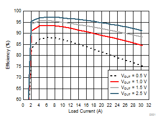
| VIN = 5 V | fSW = 500 kHz | RBOOT = 0 Ω |
| L = 470 nH | No snubber | RDCR = 0.3 mΩ |
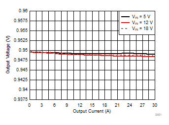
| VOUT = 0.95 V |
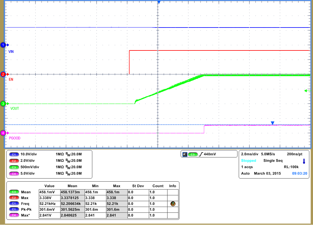
| VIN = 12 V | VOUT = 0.95 V | IOUT = 20 A |
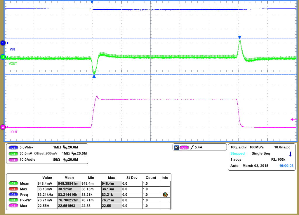
| VIN = 12 V | VOUT = 0.95 V | IOUT = 0 A to 20A , 2.5 A/µs |
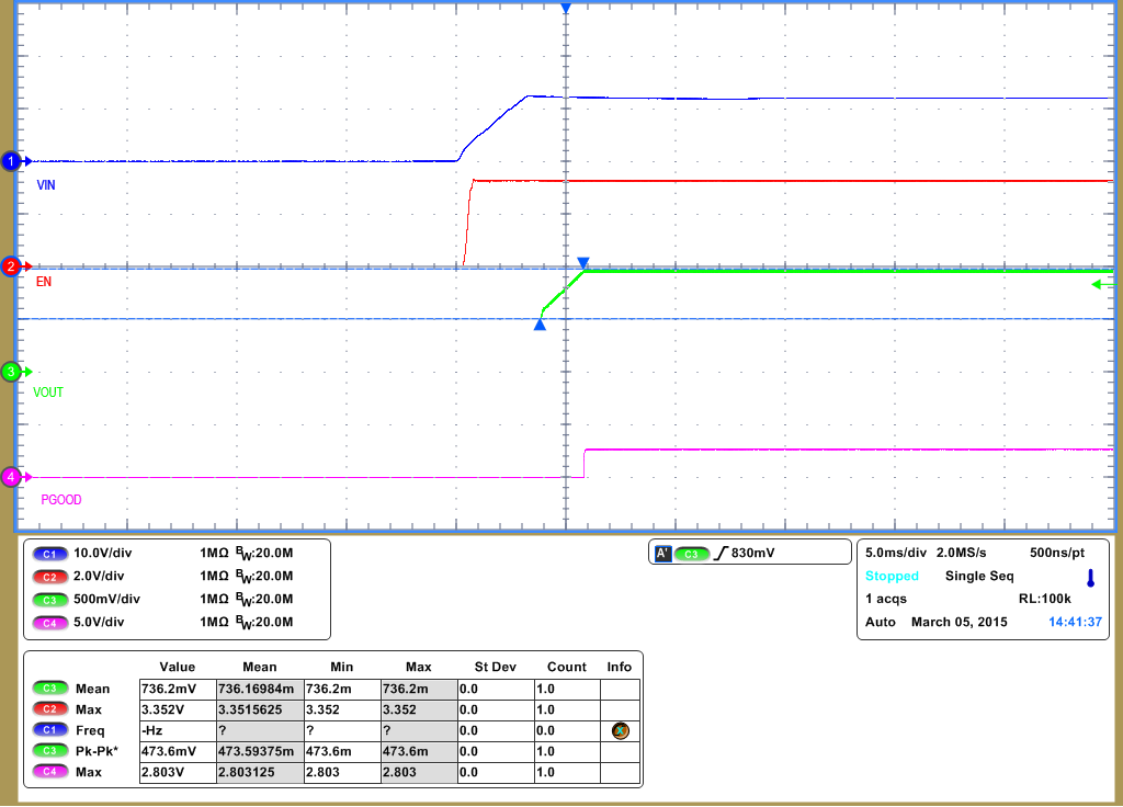
| VIN = 12 V | IOUT = 0 A | VPRE-BIAS= 0.5 V |
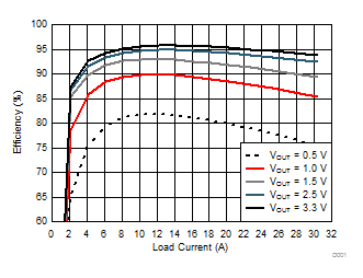
| VIN = 12 V | fSW = 500 kHz | RBOOT = 0 Ω |
| L = 470 nH | No snubber | RDCR = 0.3 mΩ |
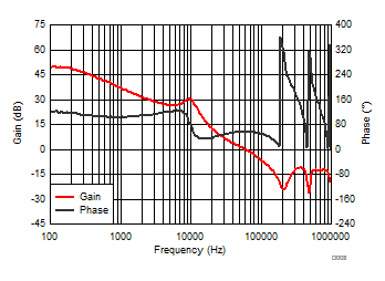
| VIN = 12 V | VOUT = 0.95 V | IOUT = 20 A |
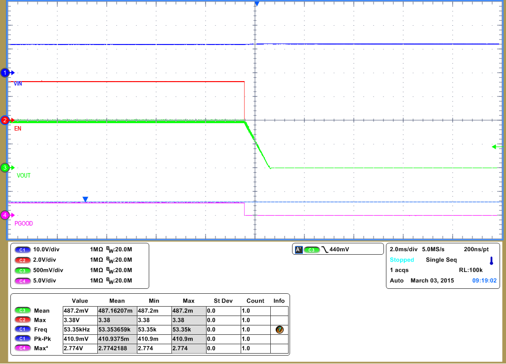
| VIN = 12 V | VOUT = 0.95 V | IOUT = 20 A |
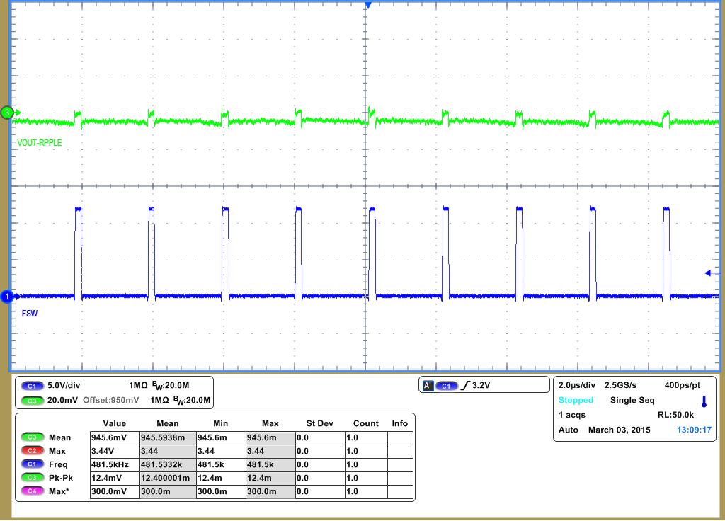
| VIN = 12 V | VOUT = 0.95 V | IOUT = 20 A |
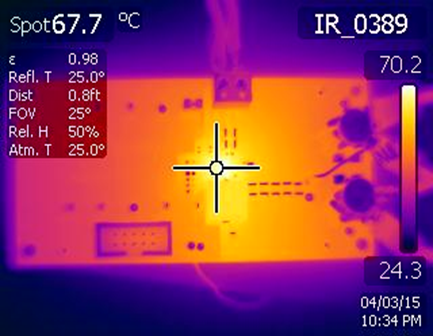
| Natural Convection | VOUT = 0.95 V | |
| VIN = 12 V | IOUT = 20 A | fSW = 500 kHz |