ZHCSCI5B May 2014 – July 2016 TPS544B20 , TPS544C20
PRODUCTION DATA.
- 1 特性
- 2 应用范围
- 3 说明
- 4 修订历史记录
- 5 Device Comparison Table
- 6 Pin Configuration and Functions
- 7 Specifications
-
8 Detailed Description
- 8.1 Overview
- 8.2 Functional Block Diagram
- 8.3
Feature Description
- 8.3.1 Turn-On and Turn-Off Delay and Sequencing
- 8.3.2 Pre-Biased Output Start-Up
- 8.3.3 Voltage Reference
- 8.3.4 Differential Remote Sense and Output Voltage Setting
- 8.3.5 PMBus Output Voltage Adjustment
- 8.3.6 Switching Frequency
- 8.3.7 Soft-Start
- 8.3.8 Linear Regulators BP3 and BP6
- 8.3.9 External Bypass (BPEXT)
- 8.3.10 Current Monitoring and Low-Side MOSFET Overcurrent Protection
- 8.3.11 High-Side MOSFET Short-Circuit Protection
- 8.3.12 Over-Temperature Protection
- 8.3.13 Input Undervoltage Lockout (UVLO)
- 8.3.14 Output Overvoltage and Undervoltage Protection
- 8.3.15 Fault Protection Responses
- 8.3.16 PMBus General Description
- 8.3.17 PMBus Address
- 8.3.18 PMBus Connections
- 8.3.19 Auto ARA (Alert Response Address) Response
- 8.4 Device Functional Modes
- 8.5 Programming
- 8.6
Register Maps
- 8.6.1 OPERATION (01h)
- 8.6.2 ON_OFF_CONFIG (02h)
- 8.6.3 CLEAR_FAULTS (03h)
- 8.6.4 WRITE_PROTECT (10h)
- 8.6.5 STORE_USER_ALL (15h)
- 8.6.6 RESTORE_USER_ALL (16h)
- 8.6.7 CAPABILITY (19h)
- 8.6.8 VOUT_MODE (20h)
- 8.6.9 VIN_ON (35h)
- 8.6.10 VIN_OFF (36h)
- 8.6.11 IOUT_CAL_OFFSET (39h)
- 8.6.12 IOUT_OC_FAULT_LIMIT (46h)
- 8.6.13 IOUT_OC_FAULT_RESPONSE (47h)
- 8.6.14 IOUT_OC_WARN_LIMIT (4Ah)
- 8.6.15 OT_FAULT_LIMIT (4Fh)
- 8.6.16 OT_WARN_LIMIT (51h)
- 8.6.17 TON_RISE (61h)
- 8.6.18 STATUS_BYTE (78h)
- 8.6.19 STATUS_WORD (79h)
- 8.6.20 STATUS_VOUT (7Ah)
- 8.6.21 STATUS_IOUT (7Bh)
- 8.6.22 STATUS_TEMPERATURE (7Dh)
- 8.6.23 STATUS_CML (7Eh)
- 8.6.24 STATUS_MFR_SPECIFIC (80h)
- 8.6.25 READ_VOUT (8Bh)
- 8.6.26 READ_IOUT (8Ch)
- 8.6.27 READ_TEMPERATURE_2 (8Eh)
- 8.6.28 PMBUS_REVISION (98h)
- 8.6.29 MFR_SPECIFIC_00 (D0h)
- 8.6.30 VREF_TRIM (MFR_SPECIFIC_04) (D4h)
- 8.6.31 STEP_VREF_MARGIN_HIGH (MFR_SPECIFIC_05) (D5h)
- 8.6.32 STEP_VREF_MARGIN_LOW (MFR_SPECIFIC_06) (D6h)
- 8.6.33 PCT_VOUT_FAULT_PG_LIMIT (MFR_SPECIFIC_07) (D7h)
- 8.6.34 SEQUENCE_TON_TOFF_DELAY (MFR_SPECIFIC_08) (D8h)
- 8.6.35 OPTIONS (MFR_SPECIFIC_21) (E5h)
- 8.6.36 MASK_SMBALERT (MFR_SPECIFIC_23) (E7h)
- 8.6.37 DEVICE_CODE (MFR_SPECIFIC_44) (FCh)
-
9 Applications and Implementation
- 9.1 Application Information
- 9.2
Typical Application
- 9.2.1 Design Requirements
- 9.2.2
Detailed Design Procedure
- 9.2.2.1 Switching Frequency Selection
- 9.2.2.2 Inductor Selection
- 9.2.2.3 Output Capacitor Selection
- 9.2.2.4 D-CAP Mode and D-CAP2 Mode Stability
- 9.2.2.5 Input Capacitor Selection
- 9.2.2.6 Bootstrap Capacitor and Resistor Selection
- 9.2.2.7 BP6, BP3 and BPEXT
- 9.2.2.8 R-C Snubber and VIN Pin High-Frequency Bypass
- 9.2.2.9 Temperature Sensor
- 9.2.2.10 Key PMBus Parameter Selection
- 9.2.2.11 Output Voltage Setting and Frequency Compensation Selection
- 9.2.3 Application Curves
- 10Power Supply Recommendations
- 11Layout
- 12器件和文档支持
- 13机械、封装和可订购信息
9 Applications and Implementation
9.1 Application Information
The TPS544B20 and TPS544C20 devices are highly-integrated synchronous step-down DC-DC converters. These devices are used to convert a higher DC input voltage to a lower DC output voltage, with a maximum output current of 20 A and 30 A respectively.
9.2 Typical Application
Use the following design procedure to select key component values for this family of devices, and set the appropriate behavioral options according to the PMBus protocol.
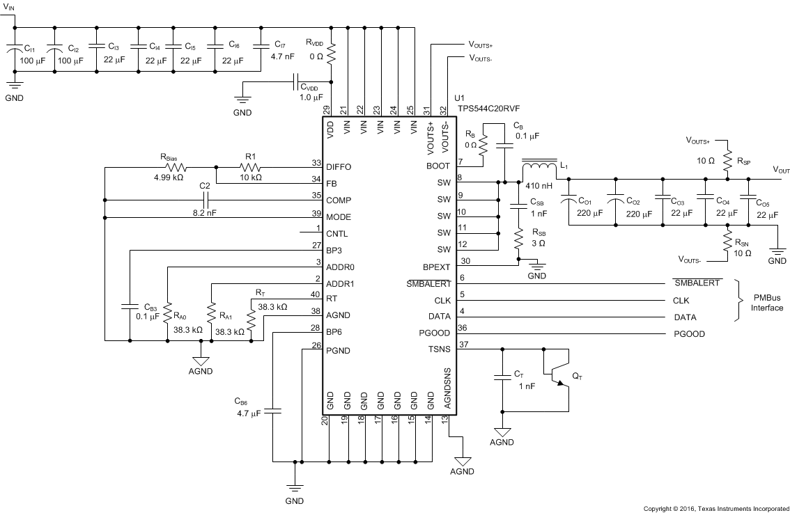 Figure 32. TPS544C20 4.5-V to 18-V Input, 1.8-V Output, 30-A Converter
9.2.1 Design Requirements
For this design example, use the following input parameters.
Table 10. Design Example Specifications
| PARAMETER | TEST CONDITION | MIN | TYP | MAX | UNIT | |
|---|---|---|---|---|---|---|
| VI | Input voltage | 4.5 | 12.0 | 18.0 | V | |
| VI(ripple) | Input ripple voltage | IOUT = 30 A | 0.4 | V | ||
| VO | Output voltage | 1.8 | V | |||
| Line regulation | 4.5 V ≤ VI ≤ 18 V | 0.5% | ||||
| Load regulation | 0 V ≤ IO ≤ 30 A | 0.5% | ||||
| V(PP) | Output ripple voltage | IO = 30 A | 18 | mV | ||
| V(OVER) | Transient response overshoot | I(STEP) = 10 A | 36 | mV | ||
| V(UNDER) | Transient response undershoot | I(STEP) = 10 A | -36 | mV | ||
| IO | Output current | 5 V ≤ VI ≤ 18 V | 0 | 20 | 30 | A |
| tSS | Soft-start time | VI = 12 V | 2.7 | ms | ||
| IOC | Overcurrent trip point | 40 | A | |||
| η | Efficiency | IO = 20 A, VI = 12 V | 90% | |||
| fSW | Switching frequency | 500 | kHz | |||
9.2.2 Detailed Design Procedure
9.2.2.1 Switching Frequency Selection
There is a trade-off between higher and lower switching frequencies. Higher switching frequencies may produce smaller a solution size using lower valued inductors and smaller output capacitors compared to a power supply that switches at a lower frequency. However, the higher switching frequency produce higher switch losses, which decrease efficiency and impact thermal performance. In this design, a moderate switching frequency of 500 kHz achieves both a balance between a small solution size and high-efficiency operation. With the frequency selected, use Table 2 to select the timing resistor. For a frequency of 500 kHz RRT is 38.2 kΩ.
9.2.2.2 Inductor Selection
To calculate the value of the output inductor, use Equation 12. The coefficient KIND represents the amount of peak-to-peak inductor ripple current relative to the maximum output current. The output capacitor filters the inductor ripple current; therefore, choosing a high inductor ripple current impacts the selection of the output capacitor because the output capacitor must have a ripple current rating equal to or greater than the inductor ripple current. To achieve balanced performance, maintain a KIND coefficient between 0.3 and 0.4. Using this target ripple current, the required inductor size can be calculated as shown in Equation 12.

Selecting KIND = 0.3, the target inductance L1 = 360 nH. Using the next standard value, the 320 nH Pulse (brand) PG077.321NL is chosen in this application for its high current rating, low DCR, and small size. The inductor ripple current, RMS current, and peak current can be calculated using Equation 13, Equation 14 and Equation 15. These values should be used to select an inductor with approximately the target inductance value, and current ratings that allow normal operation with some margin.


The Pulse PG077.321NL is rated for 45 A RMS current, and 48-A saturation. Using this inductor, the ripple current IRIPPLE= 10.1 A, the RMS inductor current IL(rms)= 30.14 A, and peak inductor current IL(peak)= 35 A.
9.2.2.3 Output Capacitor Selection
There are three primary considerations for selecting the value of the output capacitor. The output capacitor affects three criteria:
- how the regulator responds to a load transition
- the output voltage ripple
- the minimum output capacitance needed to maintain stable D-CAP2 mode control
The output capacitance needs to be selected based on the most stringent of these three criteria.
9.2.2.3.1 Response to a Load Transition
The desired response to a load transition is the first criterion. The output capacitor must supply the load with the required current when not immediately provided by the regulator. When the output capacitor supplies load current, the impedance of the capacitor greatly affects the magnitude of voltage deviation during the transient.
These devices use Adaptive Constant On-Time (COT) control. During a transient, the ON-time remains unchanged from normal operation, but the off-time shortens to allow a rapid increase in the inductor current in order to meet the demands of the load transition. To estimate the time required to respond to a load increase, calculate the number of switching cycles required to change the inductor current using Equation 16.

And estimate the time needed to produce that number of cycles during a transient as Equation 17:

The output capacitor must support the full change in output current for half of the time, so the minimum output capacitance can be estimated by Equation 18:

The output capacitor must also absorb the full change in output current for half of the time needed to remove the excess current from the inductor during a rapid load decrease. This minimum output capacitance can be estimated using Equation 19:

In order to meet the transient response requirements, the output capacitance must be greater than the larger of Cundershoot and Covershoot.
In this case, the highest minimum output capacitance (COUT(min)) to meet the response to a load transition is the overshoot requirement, which dictates the minimum output capacitance. Therefore, using Equation 19, the minimum output capacitance required to meet the transient requirement is 494 µF.
9.2.2.3.2 Output Voltage Ripple
The output voltage ripple is the second criterion. Equation 20 calculates the minimum output capacitance required to meet the output voltage ripple specification. This criterion is the requirement when the impedance of the output capacitance is dominated by ESR.

In this case, the maximum output voltage ripple is 18 mV. Under this requirement, the minimum output capacitance for ripple (as calculated in Equation 20) yields 140 μF. Because this capacitance value is smaller than the output capacitance required to meet the transient response, select the output capacitance value based on the transient requirement. For this application, two 220-µF, low-ESR polymer bulk capacitors, three 47-µF capacitors and three 22-µF ceramic capacitors are selected to meet the transient specification with at least 80% margin. Therefore COUT equals 647 µF.
With the target output capacitance value chosen, Equation 21 calculates the maximum ESR the output capacitor bank can have to meet the output voltage ripple specification. Equation 21 indicates the ESR should be less than 1.4 mΩ. The six ceramic capacitors each contribute approximately 2 mΩ, making the effective ESR of the output capacitor bank approximately 0.33 mΩ, meeting the specification with sufficient margin.

Additional capacitance de-ratings for aging, temperature and DC bias should be factored in, which increases the minimum required capacitance value. Capacitors generally have limits to the amount of ripple current they can handle without failing or producing excess heat. An output capacitor that can support the inductor ripple current must be specified. Some capacitor data sheets specify the RMS (root mean square) value of the maximum ripple current. Equation 22 can be used to calculate the RMS ripple current the output capacitor needs to support. For this application, Equation 22 yields 2.28 A.

9.2.2.4 D-CAP Mode and D-CAP2 Mode Stability
D-CAP mode control requires that the ESR ripple at the FB pin be at least 15 mV (or 2.5%) of the output voltage and the ESR-zero frequency of the output capacitor is less than 1/4 the switching frequency. Because this design requires output voltage ripple less than 2.5% of the output voltage and uses low-ESR, specialty polymer, and ceramic output capacitors, this design uses D-CAP2 mode control. Because D-CAP2 mode control uses an internally generated ramp to emulate the ESR of the output capacitor, D-CAP2 mode requires sufficient output capacitance to maintain an effective ESR-zero frequency less than 1/4 of the nominal switching frequency with this emulated ESR. The minimum capacitance for stability can be calculated in Equation 23 using τIem from Table 11:

Table 11. D-CAP2 Mode Current Emulation Time Constants
| NOMINAL FREQUENCY (kHz) | τIem(µs) |
|---|---|
| 250 | 104 |
| 300 | 98 |
| 400 | 87 |
| 500 | 76 |
| 650 | 60 |
| 750 | 52 |
| 850 | 44 |
| 1000 | 33 |
9.2.2.5 Input Capacitor Selection
The TPS544B20 and TPS544C20 devices require a capacitor with these features:
- high-quality
- ceramic
- type X5R or X7R
- input decoupling feature
- a value of 0.1 μF to 1.0 μF of effective capacitance on the VDD pin, relative to GND
The power stage input decoupling capacitance (effective capacitance at the VIN and GND pins) must be sufficient to supply the high switching currents demanded when the high-side MOSFET switches on, while providing minimal input voltage ripple as a result. This effective capacitance includes any DC bias effects. The voltage rating of the input capacitor must be greater than the maximum input voltage. The capacitor must also have a ripple current rating greater than the maximum input current ripple to the device during full load. The input ripple current can be calculated using Equation 24.

The minimum input capacitance and ESR values for a given input voltage ripple specification, VIN(ripple), are shown in Equation 25 and Equation 26. The input ripple is composed of a capacitive portion, VRIPPLE(cap), and a resistive portion, VRIPPLE(esr).


The value of a ceramic capacitor varies significantly with temperature and the amount of DC bias applied to the capacitor. The capacitance variations due to temperature can be minimized by selecting a dielectric material that is stable over temperature. X5R and X7R ceramic dielectric capacitors are usually selected for power regulator capacitors because they have a high capacitance-to-volume ratio and are fairly stable during temperature changes. The input capacitor must also be selected with the DC bias taken into account. To support the maximum input voltage, this design requires a ceramic capacitor with a rating of at least 25 V. Allow 0.1-V input ripple for VRIPPLE(cap), and 0.3-V input ripple for VRIPPLE(esr). Using Equation 25 and Equation 26, the minimum input capacitance for this design is 60 µF, and the maximum ESR is 2.8 mΩ. Four 22-μF, 25-V ceramic capacitors and two additional 100-μF, 25-V low-ESR polymer capacitors in parallel were selected for the power stage. For the VDD pin, one 1.0-μF, 25-V ceramic capacitor was selected. The input voltage (VIN) and power input voltage (PVIN) pins must be tied together. The input capacitance value determines the input ripple voltage of the regulator. Using the design example values, IOUT(max) = 30 A, CIN = 288 μF, fSW = 500 kHz, yields a maximum RMS input ripple current of 14.7 Arms.
9.2.2.6 Bootstrap Capacitor and Resistor Selection
A ceramic capacitor with a value of 0.1 μF must be connected between the BOOT and SW pins for proper operation. It is recommended to use a ceramic capacitor with X5R or better grade dielectric. The capacitor should have voltage rating of 25 V or higher. To reduce the dV/dt of the rising edge of the SW node, reduce ringing and EMI, a resistor RBOOT up to 5 Ω can be placed in series with the bootstrap capacitor.
9.2.2.7 BP6, BP3 and BPEXT
This design does not include an auxiliary 5-V supply, so BPEXT is terminated to GND. According to the recommendations in , BP3 is bypassed to AGND with 100 nF of capacitance, and BP6 is bypassed to GND with 4.7-µF of capacitance. In order for the regulator to function properly, it is important that these capacitors be located close to the TPS544C20, with low-impedance return paths to AGND or GND as appropriate. See Figure 45 for more information.
9.2.2.8 R-C Snubber and VIN Pin High-Frequency Bypass
Although it is possible to operate the TPS544C20 within absolute maximum ratings without including any ringing reduction techniques, some designs may require external components to further reduce ringing levels. This example uses two approaches:
- a high frequency power stage bypass capacitor on the VIN pins
- an R-C snubber between the SW and GND
Including a high-frequency bypass capacitor is a lossless ringing reduction technique which helps minimizes the outboard parasitic inductances in the power stage. These capacitors store energy during the low-side MOSFET on-time, and discharge once the high-side MOSFET is turned on. For this example a 4.7-nF, 25-V, 0402 sized high-frequency capacitor is selected. The placement of this capacitor (shown in Figure 46) is critical to its effectiveness.
Additionally, an R-C snubber circuit is added to this example. To balance efficiency and spike levels, a 1-nF capacitor and a 3-Ω resistor are chosen. In this example an 0805 resistor is chosen, which is rated for 0.125 W, nearly twice the estimated power dissipation. Figure 33 and Figure 34 show the effect of the R-C snubber on the rising edge of the SW pin. See SLUP100 for more information about snubber circuits.
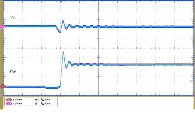
| VIN = 12 V | IOUT = 20 A | Snubber = 1nF + 3Ω |
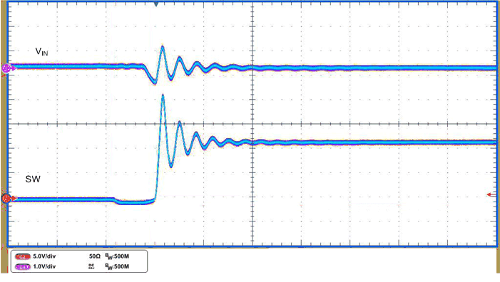
| VIN = 12 V | IOUT = 20 A | Snubber = Open |
9.2.2.9 Temperature Sensor
This application design uses a surface-mount MMBT3904SL for the temperature sensor, QT. In this example, the sensor monitors the PCB temperature where it is generally the highest, next to the power inductor. Placement of the temperature sensor and routing back to the TSNS pin are critical design features to reduce noise its temperature measurements. In this example, the temperature sensor is placed on the VOUT side of the power inductor to avoid switching noise from the SW plane, and routed back to the TSNS and AGND pin. Additionally, a 330-pF capacitor, CT, is placed from TSNS to AGND near the TSNS pin.
Disable external temperature sensing by terminating TSNS to AGND with a 0-Ω resistor. This termination forces the temperature readings to –40 °C, and prevents external over-temperature fault trips.
9.2.2.10 Key PMBus Parameter Selection
Several of the key design parameters for the TPS544B20 and TPS544C20 device can be configured according to the PMBus protocol, and stored to its non-volatile memory (NVM) for future use.
9.2.2.10.1 Enable, UVLO and Sequencing
Use the ON_OFF_CONFIG (02h) command to select the turn-on behavior of the converter. For this example, the CNTL pin was used to enable or disable the converter, regardless of the state of OPERATION (01h), as long as input voltage is present, and above the UVLO threshold.
The minimum input voltage, VIN(min) , for this example is 4.5 V. The VIN_ON command was set to 4.25 V, and the VIN_OFF command was set to 4.0 V, giving 250 mV of hysteresis. If VIN falls below VIN_OFF, power conversion stops, until it is raised above VIN_ON.
This example lacks specific turn-on or turn-off delay requirements, so SEQUENCE_TON_TOFF_DELAY was used to set both the turn-on and turn-off delays to 0 × the soft-start time, the delay between enabling power conversion, and the rise of the output voltage is approximately 400 µs. See the Soft-Start section for more information.
9.2.2.10.2 Soft-Start Time
The TON_RISE command sets the soft-start time. When selecting the soft-start time, consider the charging current for the output capacitors. In some applications (for example those with large amounts of output capacitance) this current can lead to problems with nuisance tripping of the overcurrent protection circuitry. To avoid nuisance tripping, the output capacitor charging current should be included when choosing a soft-start time, and overcurrent threshold. The capacitor charging current can be calculated using Equation 27.

After calculating the charging current, the overcurrent threshold can then be calibrated to the sum of the maximum load current and the output capacitor charging current plus some margin.
In this example, the soft-start time is arbitrarily selected to be the default value, 2.7 ms. In this case, the charging current, ICAP = 337 mA.
9.2.2.10.3 Overcurrent Threshold and Response
The IOUT_OC_FAULT_LIMIT command sets the overcurrent threshold. The current limit should be set to the maximum load current, plus the output capacitor charging current during start-up, plus some margin for load transitions and component variation. The amount of margin required depends on the individual application, but a suggested starting point is 30%. More or less may be required. For this application, the maximum load current is 30 A, the output capacitor charging current is 337 mA. This design uses the factory default overcurrent threshold of 39 A.
The IOUT_OC_FAULT_RESPONSE command sets the desired response to an overcurrent event. In this example, the converter is configured to latch-off in the event of an overcurrent. TPS544C20 device can also be configured to hiccup, (continuously restart waiting for a 7 x soft-start time-out between re-trials. )
9.2.2.10.4 Power Good, Output Overvoltage and Undervoltage Protection
The PCT_VOUT_FAULT_PG_LIMIT command configures the PGOOD, and regulation windows. This example includes a moderate threshold setting. The resulting power good window is ±12.5%, and the resulting overvoltage and undervoltage window is ±16.8%. More or less aggressive protection levels can be selected according to the PMBus protocol.
9.2.2.11 Output Voltage Setting and Frequency Compensation Selection
A feedback divider from DIFFO to AGND sets the output voltage. This design arbitrarily selects an R1 value of 20 kΩ. Using R1 and the desired output voltage, and calculate RBIAS using Equation 28 to be 10 kΩ.

The TPS544B20 and TPS544C20 devices use D-CAP2 mode control with a transconductance error amplifier to eliminate the output voltage error introduced by valley voltage regulation. To stabilize the error amplifer, TI recommends a 10-nF capacitor from COMP to AGND. To improve transient response and increase phase margin, a series resistor, RCOMP, can be added. When using RCOMP, add a 1.0-nF capacitor from COMP to AGND to limit the error amplifier gain at high frequency. Use Equation 29 to calculate the value of RCOMP.

Alternatively, for output voltages 1.2 V and higher, a feedforward capacitor, C1, can be added in parallel with R1 from DIFFO to FB to provide similar improvement to transient response and phase margin. Use Equation 30 to calculate the value of C1.

The resulting design example frequency compensation values are:
- R1 = 20 kΩ
- RBIAS = 10 kΩ
- C1 = 420 pF
9.2.3 Application Curves
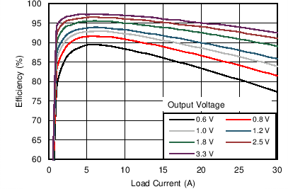
| VIN = 5 V | fSW = 500 kHz | TA = 25 °C |
| L = 410 nH | Snubber = Open | RBOOT = 0 Ω |
| RDCR = 0.3 mΩ |
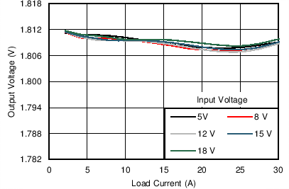
| VIN = 12 V |
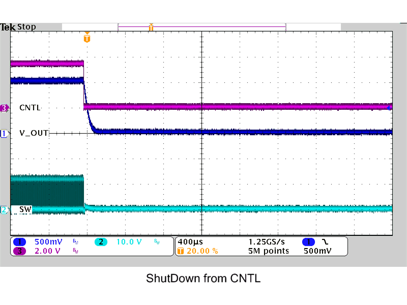
| VIN = 12 V | IOUT = 20 A |
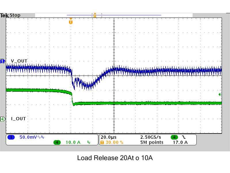
| VIN = 12 V | IOUT = 20 A | tFALL = 2.0 µs |
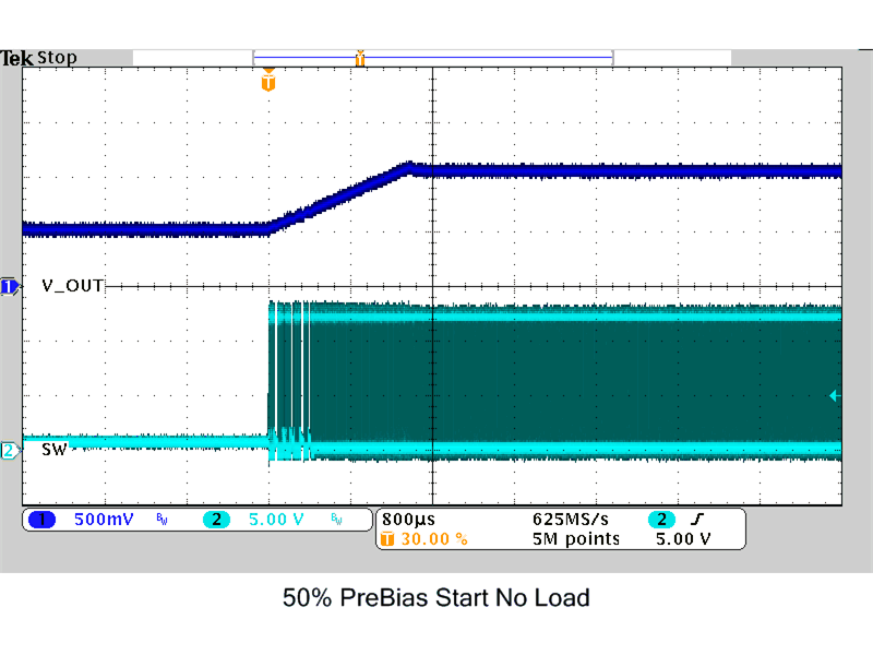
| VIN = 12 V | IOUT = 0 A | VPRE-BIAS= 900 mV |
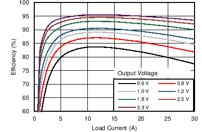
| VIN = 12 V | fSW = 500 kHz | TA = 25 °C |
| L = 410 nH | Snubber = Open | RBOOT = 0 Ω |
| RDCR = 0.3 mΩ |
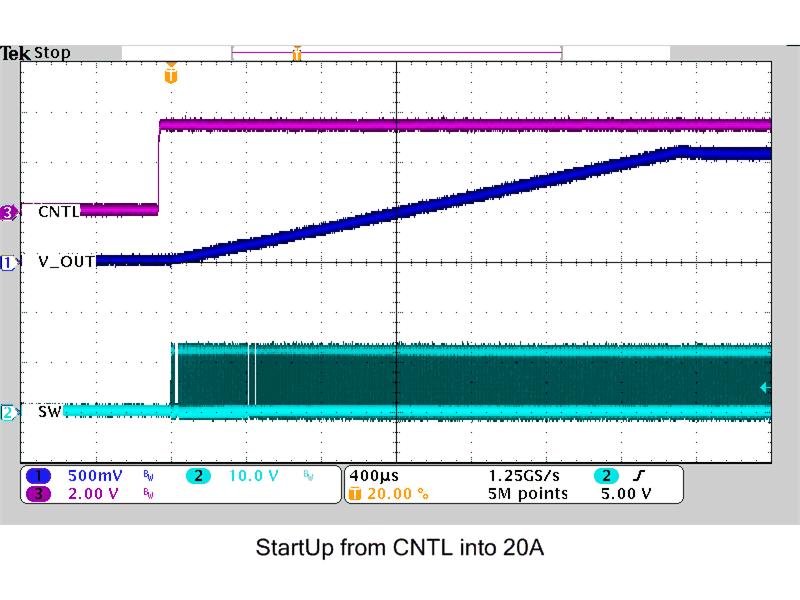
| VIN = 12 V | IOUT = 20 A |
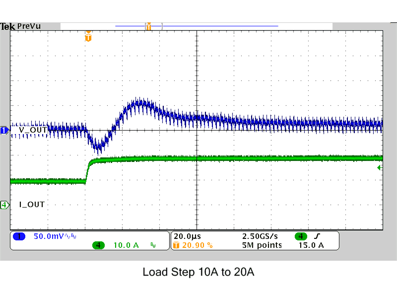
| VIN = 12 V | IOUT = 20 A | tRISE = 2.0 µs |
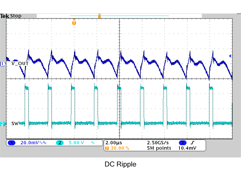
| VIN = 12 V | IOUT = 20 A |
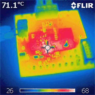
| Natural Convection | ||
| VIN = 12 V | IOUT = 20 A | fSW = 500 kHz |