ZHCSJY4B July 2008 – June 2019 TPS5450-Q1
PRODUCTION DATA.
- 1 特性
- 2 应用
- 3 说明
- 4 修订历史记录
- 5 Pin Configuration and Functions
- 6 Specifications
-
7 Detailed Description
- 7.1 Overview
- 7.2 Functional Block Diagram
- 7.3
Feature Description
- 7.3.1 Oscillator Frequency
- 7.3.2 Voltage Reference
- 7.3.3 Enable (ENA) and Internal Slow Start
- 7.3.4 Undervoltage Lockout (UVLO)
- 7.3.5 Output Feedback (VSENSE) and Internal Compensation
- 7.3.6 Voltage Feedforward
- 7.3.7 Pulse-Width-Modulation (PWM) Control
- 7.3.8 Overcurrent Limiting
- 7.3.9 Overvoltage Protection
- 7.3.10 Thermal Shutdown
-
8 Application Information
- 8.1 Application Information
- 8.2
Typical Application
- 8.2.1 Design Requirements
- 8.2.2
Detailed Design Procedure
- 8.2.2.1 Custom Design With WEBENCH® Tools
- 8.2.2.2 Boost Capacitor (BOOT)
- 8.2.2.3 Switching Frequency
- 8.2.2.4 Input Capacitors
- 8.2.2.5 Output Filter Components
- 8.2.2.6 Output Voltage Setpoint
- 8.2.2.7 Boot Capacitor
- 8.2.2.8 Catch Diode
- 8.2.2.9 Output Voltage Limitations
- 8.2.2.10 Internal Compensation Network
- 8.2.3 Application Curves
- 9 Layout
- 10器件和文档支持
- 11机械、封装和可订购信息
5 Pin Configuration and Functions
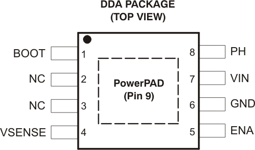
DDA Package
8-Pin SO PowerPAD
Top View

Pin Functions
| PIN | DESCRIPTION | |
|---|---|---|
| NAME | NO. | |
| BOOT | 1 | Boost capacitor for the high-side FET gate driver. Connect 0.01-μF low-ESR capacitor from BOOT pin to PH pin. |
| NC | 2, 3 | No internal connection |
| VSENSE | 4 | Feedback voltage for the regulator. Connect to output voltage divider. |
| ENA | 5 | On/off control. Below 0.5 V, the device stops switching. Float the pin to enable. |
| GND | 6 | Ground. Connect to thermal pad. |
| VIN | 7 | Input supply voltage. Bypass VIN pin to GND pin close to device package with a high-quality low-ESR ceramic capacitor. |
| PH | 8 | Source of the high side power MOSFET. Connected to external inductor and diode. |
| PowerPAD | 9 | GND pin must be connected to the exposed pad for proper operation. |