ZHCS924D May   2012  – April 2021 TPS54526

PRODUCTION DATA  

  1. 特性
  2. 应用
  3. 说明
  4. Revision History
  5. Pin Configuration and Functions
  6. Specifications
    1. 6.1 Absolute Maximum Ratings
    2. 6.2 Handling Ratings
    3. 6.3 Recommended Operating Conditions
    4. 6.4 Thermal Information
    5. 6.5 Electrical Characteristics
    6. 6.6 Timing Requirements
    7. 6.7 Typical Characteristics
  7. Detailed Description
    1. 7.1 Overview
    2. 7.2 Functional Block Diagram
    3. 7.3 Feature Description
      1. 7.3.1  PWM Operation
      2. 7.3.2  PWM Frequency and Adaptive On-Time Control
      3. 7.3.3  Soft Start and Pre-Biased Soft Start
      4. 7.3.4  Power Good
      5. 7.3.5  VREG5
      6. 7.3.6  Output Discharge Control
      7. 7.3.7  Current Protection
      8. 7.3.8  Over/Under Voltage Protection
      9. 7.3.9  UVLO Protection
      10. 7.3.10 Thermal Shutdown
    4. 7.4 Device Functional Modes
      1. 7.4.1 Auto-Skip Eco-Mode™ Control
  8. Application and Implementation
    1. 8.1 Application Information
    2. 8.2 Typical Application
      1. 8.2.1 Design Requirements
      2. 8.2.2 Detailed Design Procedure
        1. 8.2.2.1 Step By Step Design Procedure
        2. 8.2.2.2 Output Voltage Resistors Selection
        3. 8.2.2.3 Output Filter Selection
        4. 8.2.2.4 Input Capacitor Selection
        5. 8.2.2.5 Bootstrap Capacitor Selection
        6. 8.2.2.6 VREG5 Capacitor Selection
      3. 8.2.3 Application Curve
  9. Power Supply Recommendations
  10. 10Layout
    1. 10.1 Layout Guidelines
    2. 10.2 Layout Example
  11. 11Device and Documentation Support
    1. 11.1 接收文档更新通知
    2. 11.2 支持资源
    3. 11.3 Trademarks
    4. 11.4 静电放电警告
    5. 11.5 术语表
  12. 12Mechanical, Packaging, and Orderable Information
    1. 12.1 Thermal Information

封装选项

机械数据 (封装 | 引脚)
散热焊盘机械数据 (封装 | 引脚)
订购信息

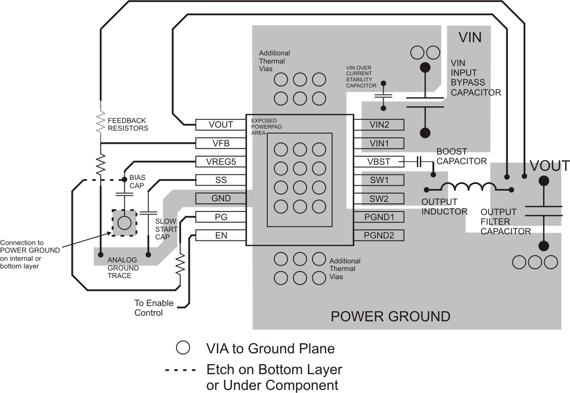
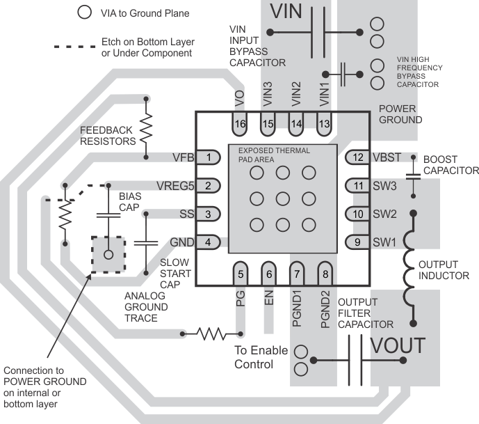
Layout Example

GUID-CE267723-5EA8-4CBD-A292-56724A6EB081-low.gifFigure 10-1 PCB Layout for PWP Package
GUID-8B29F7A9-BF2C-443A-AF0E-DE9BAE01E6F8-low.gifFigure 10-2 PCB Layout for RSA Package