ZHCSB15B May 2013 – October 2023 TPS54531
PRODUCTION DATA
- 1
- 1 特性
- 2 应用
- 3 说明
- 4 Revision History
- 5 Pin Configuration and Functions
- 6 Specifications
-
7 Detailed Description
- 7.1 Overview
- 7.2 Functional Block Diagram
- 7.3
Feature Description
- 7.3.1 Fixed-Frequency PWM Control
- 7.3.2 Voltage Reference (Vref)
- 7.3.3 Bootstrap Voltage (BOOT)
- 7.3.4 Enable and Adjustable Input Undervoltage Lockout (VIN UVLO)
- 7.3.5 Programmable Slow Start Using SS Pin
- 7.3.6 Error Amplifier
- 7.3.7 Slope Compensation
- 7.3.8 Current-Mode Compensation Design
- 7.3.9 Overcurrent Protection and Frequency Shift
- 7.3.10 Overvoltage Transient Protection
- 7.3.11 Thermal Shutdown
- 7.4 Device Functional Modes
-
8 Application and Implementation
- 8.1 Application Information
- 8.2
Typical Application
- 8.2.1 Design Requirements
- 8.2.2
Detailed Design Procedure
- 8.2.2.1 Custom Design With WEBENCH® Tools
- 8.2.2.2 Switching Frequency
- 8.2.2.3 Output Voltage Set Point
- 8.2.2.4 Undervoltage Lockout Set Point
- 8.2.2.5 Input Capacitors
- 8.2.2.6 Output Filter Components
- 8.2.2.7 Compensation Components
- 8.2.2.8 Bootstrap Capacitor
- 8.2.2.9 Catch Diode
- 8.2.2.10 Slow-Start Capacitor
- 8.2.2.11 Output Voltage Limitations
- 8.2.2.12 Power Dissipation Estimate
- 8.2.3 Application Curves
- 8.3 Power Supply Recommendations
- 8.4 Layout
- 9 Device and Documentation Support
- 10Mechanical, Packaging, and Orderable Information
8.2.2.7 Compensation Components
Several possible methods exist to design closed loop compensation for DC/DC converters. For the ideal current mode control, the design equations can be easily simplified. The power stage gain is constant at low frequencies, and rolls off at –20 dB/decade above the modulator pole frequency. The power stage phase is 0 degrees at low frequencies and begins to fall one decade below the modulator pole frequency reaching a minimum of –90 degrees one decade above the modulator pole frequency. Use Equation 16 to calculate the modulator pole frequency.
For the TPS54531 device, most circuits have relatively high amounts of slope compensation. As more slope compensation is applied, the power stage characteristics deviate from the ideal approximations. The phase loss of the power stage now approaches –180 degrees, making compensation more difficult. The power stage transfer function can be solved but requires a tedious calculation. Use the PSpice model to accurately model the power-stage gain and phase so that a reliable compensation circuit can be designed. Alternately, a direct measurement of the power stage characteristics can be used. That is the technique used in this design procedure. For this design, the calculate values are as follows:
L1 = 4.7 µH
C8 and C9 = 47 µF (each)
ESR = 3 mΩ
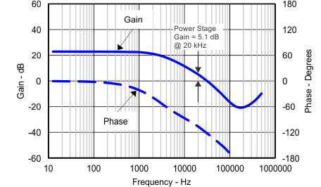
Figure 8-2 shows the power stage characteristics.
 Figure 8-2 Power
Stage Gain and Phase Characteristics
Figure 8-2 Power
Stage Gain and Phase CharacteristicsFor this design, the intended crossover frequency is 20 kHz. From the power stage gain and phase plots, the gain at 20 kHz is 5.1 dB and the phase is about –100 degrees. For 60 degrees of phase margin, additional phase boost from a feed-forward capacitor in parallel with the upper resistor of the voltage set point divider is not needed. R3 sets the gain of the compensated error amplifier to be equal and opposite the power stage gain at crossover. Use Equation 17 to calculate the required value of R3.
To maximize phase gain, the compensator zero is placed one decade below the crossover frequency of 20 kHz. Use Equation 18 to calculate the required value for C6.
To maximize phase gain the high frequency pole is placed one decade above the crossover frequency of 20 kHz. The pole can also be useful to offset the ESR of aluminum electrolytic output capacitors. Use Equation 19 to calculate the value for C7.
For this design, the calculated values are as follows:
R3 = 37.4 kΩ
C6 = 2200 pF
C7 = 22 pF