ZHCSCT5A September 2014 – January 2017 TPS54561-Q1
PRODUCTION DATA.
- 1 特性
- 2 应用范围
- 3 说明
- 4 修订历史记录
- 5 Pin Configuration and Functions
- 6 Specifications
-
7 Detailed Description
- 7.1 Overview
- 7.2 Functional Block Diagram
- 7.3
Feature Description
- 7.3.1 Fixed-Frequency PWM Control
- 7.3.2 Slope Compensation Output Current
- 7.3.3 Pulse-Skipping Eco-mode Control Scheme
- 7.3.4 Low-Dropout Operation and Bootstrap Voltage (BOOT)
- 7.3.5 Error Amplifier
- 7.3.6 Adjusting the Output Voltage
- 7.3.7 Enable and Adjust Undervoltage Lockout
- 7.3.8 Soft-Start and Tracking Pin (SS/TR)
- 7.3.9 Sequencing
- 7.3.10 Constant Switching Frequency and Timing Resistor (RT/CLK Pin)
- 7.3.11 Accurate Current-Limit Operation and Maximum Switching Frequency
- 7.3.12 Synchronization to RT/CLK Pin
- 7.3.13 Power Good (PWRGD Pin)
- 7.3.14 Overvoltage Protection
- 7.3.15 Thermal Shutdown
- 7.3.16 Small-Signal Model for Loop Response
- 7.3.17 Simplified Small-Signal Model for Peak-Current-Mode Control
- 7.3.18 Small-Signal Model for Frequency Compensation
- 7.4 Device Functional Modes
-
8 Application and Implementation
- 8.1 Application Information
- 8.2
Typical Application
- 8.2.1 Design Requirements
- 8.2.2
Detailed Design Procedure
- 8.2.2.1 Custom Design with WEBENCH® Tools
- 8.2.2.2 Selecting the Switching Frequency
- 8.2.2.3 Output Inductor Selection (L(O))
- 8.2.2.4 Output Capacitor
- 8.2.2.5 Catch Diode
- 8.2.2.6 Input Capacitor
- 8.2.2.7 Soft-Start Capacitor
- 8.2.2.8 Bootstrap Capacitor Selection
- 8.2.2.9 Undervoltage Lockout Set Point
- 8.2.2.10 Output Voltage and Feedback Resistor Selection
- 8.2.2.11 Compensation
- 8.2.2.12 Discontinuous Conduction Mode and Eco-mode Boundary
- 8.2.2.13 Power Dissipation Estimate
- 8.2.3 Safe Operating Area
- 8.2.4 Application Curves
- 8.2.5 Inverting Power Supply
- 8.2.6 Split-Rail Power Supply
- 9 Power Supply Recommendations
- 10Layout
- 11器件和文档支持
- 12机械、封装和可订购信息
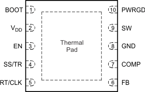
5 Pin Configuration and Functions
DPR Package
10-Pin WSON
(Top View)

Pin Functions
| PIN | I/O | DESCRIPTION | ||
|---|---|---|---|---|
| NAME | NO. | |||
| BOOT | 1 | O | The device requires a bootstrap capacitor between BOOT and SW. If the voltage on this capacitor is below the minimum required voltage to operate the high-side MOSFET, the gate driver switches off until the bootstrap capacitor recharges. | |
| COMP | 7 | O | Error amplifier output, and input to the output switch-current comparator (PWM comparator). Connect frequency compensation components to this pin. | |
| EN | 3 | I | Enable pin, with internal pullup current source. Pull below 1.2 V to disable. Float to enable. Adjust the input undervoltage lockout with two resistors. See the Enable and Adjust Undervoltage Lockout section. | |
| FB | 6 | I | Inverting input of the transconductance (gm) error amplifier. | |
| GND | 8 | — | Ground | |
| PWRGD | 10 | O | Power-good is an open-drain output that asserts if the output voltage is low because of thermal shutdown, dropout, overvoltage, or EN shutdown. | |
| RT/CLK | 5 | I | Resistor timing and external clock. An internal amplifier holds this pin at a fixed voltage when using an external resistor to ground to set the switching frequency. When pulled above the PLL upper threshold, a mode change occurs, and the pin becomes a synchronization input. This change disables the internal amplifier, and the pin is a high-impedance clock input to the internal PLL. Stopping the clocking edges re-enables the internal amplifier, and the operating mode returns to resistor programmed mode. | |
| SS/TR | 4 | I | Soft-start and tracking input pin. An external capacitor connected to this pin sets the output rise time. A voltage on this pin overrides the internal reference, which allows use of the pin for tracking and sequencing. | |
| SW | 9 | I | The source of the internal high-side power MOSFET, and switching node of the converter. | |
| VDD | 2 | I | Input supply pin with 4.5-V to 60-V operating range. | |
| Thermal pad | — | — | To ensure proper operation, electrically connect the GND pin to the copper pad under the IC on the printed circuit board. | |