ZHCSCT5A September 2014 – January 2017 TPS54561-Q1
PRODUCTION DATA.
- 1 特性
- 2 应用范围
- 3 说明
- 4 修订历史记录
- 5 Pin Configuration and Functions
- 6 Specifications
-
7 Detailed Description
- 7.1 Overview
- 7.2 Functional Block Diagram
- 7.3
Feature Description
- 7.3.1 Fixed-Frequency PWM Control
- 7.3.2 Slope Compensation Output Current
- 7.3.3 Pulse-Skipping Eco-mode Control Scheme
- 7.3.4 Low-Dropout Operation and Bootstrap Voltage (BOOT)
- 7.3.5 Error Amplifier
- 7.3.6 Adjusting the Output Voltage
- 7.3.7 Enable and Adjust Undervoltage Lockout
- 7.3.8 Soft-Start and Tracking Pin (SS/TR)
- 7.3.9 Sequencing
- 7.3.10 Constant Switching Frequency and Timing Resistor (RT/CLK Pin)
- 7.3.11 Accurate Current-Limit Operation and Maximum Switching Frequency
- 7.3.12 Synchronization to RT/CLK Pin
- 7.3.13 Power Good (PWRGD Pin)
- 7.3.14 Overvoltage Protection
- 7.3.15 Thermal Shutdown
- 7.3.16 Small-Signal Model for Loop Response
- 7.3.17 Simplified Small-Signal Model for Peak-Current-Mode Control
- 7.3.18 Small-Signal Model for Frequency Compensation
- 7.4 Device Functional Modes
-
8 Application and Implementation
- 8.1 Application Information
- 8.2
Typical Application
- 8.2.1 Design Requirements
- 8.2.2
Detailed Design Procedure
- 8.2.2.1 Custom Design with WEBENCH® Tools
- 8.2.2.2 Selecting the Switching Frequency
- 8.2.2.3 Output Inductor Selection (L(O))
- 8.2.2.4 Output Capacitor
- 8.2.2.5 Catch Diode
- 8.2.2.6 Input Capacitor
- 8.2.2.7 Soft-Start Capacitor
- 8.2.2.8 Bootstrap Capacitor Selection
- 8.2.2.9 Undervoltage Lockout Set Point
- 8.2.2.10 Output Voltage and Feedback Resistor Selection
- 8.2.2.11 Compensation
- 8.2.2.12 Discontinuous Conduction Mode and Eco-mode Boundary
- 8.2.2.13 Power Dissipation Estimate
- 8.2.3 Safe Operating Area
- 8.2.4 Application Curves
- 8.2.5 Inverting Power Supply
- 8.2.6 Split-Rail Power Supply
- 9 Power Supply Recommendations
- 10Layout
- 11器件和文档支持
- 12机械、封装和可订购信息
6 Specifications
6.1 Absolute Maximum Ratings(1)
Over operating free-air temperature range (unless otherwise noted)
(1) Stresses beyond those listed under Absolute Maximum Ratings may cause permanent damage to the device. These are stress ratings only, and do not imply functional operation of the device at these or any other conditions beyond those indicated under Rec–65ommended Operating Conditions. Exposure to absolute-maximum-rated conditions for extended periods may affect device reliability.
6.2 ESD Ratings
| VALUE | UNIT | ||||
|---|---|---|---|---|---|
| V(ESD) | Electrostatic discharge | Human-body model (HBM), per AEC Q100-002(1) | ±2000 | V | |
| Charged-device model (CDM), per AEC-Q100-011 | ±750 | ||||
(1) AEC Q100-002 indicates HBM stressing is done in accordance with the ANSI/ESDA/JEDEC JS-001 specification.
6.3 Recommended Operating Conditions
Over operating free-air temperature range (unless otherwise noted)| MIN | MAX | UNIT | |||
|---|---|---|---|---|---|
| VDD | Supply input voltage | 4.5 | 60 | V | |
| VO | Output voltage | 0.8 | 58.8 | V | |
| IO | Output current | 0 | 5 | A | |
| TJ | Junction temperature | –40 | 150 | °C | |
6.4 Thermal Information
| THERMAL METRIC(1)(2) | TPS54561-Q1 | UNIT | |
|---|---|---|---|
| DPR | |||
| 10 PINS | |||
| RθJA | Junction-to-ambient thermal resistance (standard board) | 35.1 | °C/W |
| RθJCtop | Junction-to-case (top) thermal resistance | 34.1 | °C/W |
| RθJB | Junction-to-board thermal resistance | 12.3 | °C/W |
| ψJT | Junction-to-top characterization parameter | 0.3 | °C/W |
| ψJB | Junction-to-board characterization parameter | 12.5 | °C/W |
| RθJCbot | Junction-to-case (bottom) thermal resistance | 2.2 | °C/W |
(1) For more information about traditional and new thermal metrics, see the Semiconductor and IC Package Thermal Metrics application report.
(2) Determination of the power rating at a specific ambient temperature must be at the maximum junction temperature of 150°C. This is the point where distortion starts to increase substantially. See the power dissipation estimate in the Power Dissipation Estimate section of this data sheet for more information.
6.5 Electrical Characteristics
TJ = –40°C to 150°C, VDD = 4.5 to 60 V (unless otherwise noted)| PARAMETER | TEST CONDITIONS | MIN | TYP | MAX | UNIT | ||
|---|---|---|---|---|---|---|---|
| SUPPLY VOLTAGE (VDD PIN) | |||||||
| Operating input voltage | 4.5 | 60 | V | ||||
| Internal undervoltage lockout threshold | VDD rising | 4.1 | 4.3 | 4.48 | V | ||
| Internal undervoltage lockout threshold hysteresis | 325 | mV | |||||
| Shutdown supply current | V(EN) = 0 V, TA = 25°C, 4.5 V ≤ VDD ≤ 60 V | 2.25 | 4.5 | µA | |||
| Operating: nonswitching supply current | V(FB) = 0.9 V, TA = 25°C | 152 | 200 | ||||
| ENABLE AND UVLO (EN PIN) | |||||||
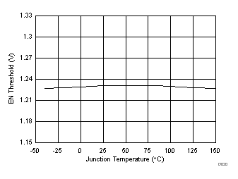
| V(EN)th | Enable threshold voltage | No voltage hysteresis, rising and falling | 1.1 | 1.2 | 1.3 | V | |
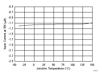
| Input current | Enable threshold + 50 mV | –4.6 | µA | ||||
| Enable threshold – 50 mV | –0.58 | –1.2 | -1.8 | ||||
| I(HYS) | Hysteresis current | –2.2 | –3.4 | -4.5 | µA | ||
| VOLTAGE REFERENCE | |||||||
| Vref | Voltage reference | 0.792 | 0.8 | 0.808 | V | ||
| HIGH-SIDE MOSFET | |||||||
| On-resistance | VDD = 12 V, V(BOOT-SW) = 6 V | 87 | 185 | mΩ | |||
| ERROR AMPLIFIER | |||||||
| Input current | 50 | nA | |||||
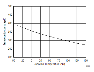
| gm(ea) | Error-amplifier transconductance | –2 µA < I(COMP) < 2 µA, V(COMP) = 1 V | 350 | µS | |||
| Error-amplifier transconductance (gm) during soft-start | –2 µA < I(COMP) < 2 µA, V(COMP) = 1 V, V(FB) = 0.4 V | 78 | µS | ||||
| A(OL) | Error-amplifier open-loop dc gain | V(FB) = 0.8 V | 10 000 | V/V | |||
| Minnimum unity-gain bandwidth | 2500 | kHz | |||||
| Error-amplifier source and sink | V(COMP) = 1 V, 100 mV overdrive | ±30 | µA | ||||
| gm(ps) | COMP to SW current transconductance | 17 | S | ||||
| CURRENT LIMIT | |||||||
| Current limit threshold | All VDD and temperatures, open loop(1) | 6.3 | 7.5 | 8.8 | A | ||
| All temperatures, VDD = 12 V, open loop(1) | 6.3 | 7.5 | 8.3 | ||||
| VDD = 12 V, TA = 25°C, open loop(1) | 7.1 | 7.5 | 7.9 | ||||
| THERMAL SHUTDOWN | |||||||
| Thermal shutdown | 176 | °C | |||||
| Thermal shutdown hysteresis | 12 | °C | |||||
| EXTERNAL CLOCK (RT/CLK PIN) | |||||||
| RT/CLK high threshold | 1.55 | 2 | V | ||||
| RT/CLK low threshold | 0.5 | 1.2 | V | ||||
| SOFT-START AND TRACKING (SS/TR PIN) | |||||||
| I(SS) | Charge current | V(SS/TR) = 0.4 V | 1.7 | µA | |||
| SS/TR-to-FB matching | V(SS/TR) = 0.4 V | 42 | mV | ||||
| SS/TR-to-reference crossover | 98% of nominal FB voltage | 1.16 | V | ||||
| SS/TR discharge current (overload) | V(FB) = 0 V, V(SS/TR) = 0.4 V | 354 | µA | ||||
| SS/TR discharge voltage | V(FB) = 0 V | 54 | mV | ||||
| POWER GOOD (PWRGD PIN) | |||||||
| FB threshold for PWRGD low | FB falling | 91% | |||||
| FB threshold for PWRGD high | FB rising | 93% | |||||
| FB threshold for PWRGD low | FB rising | 108% | |||||
| FB threshold for PWRGD high | FB falling | 106% | |||||
| Hysteresis | FB falling | 2% | |||||
| Output-high leakage | V(PWRGD) = 5.5 V, TA = 25°C | 10 | nA | ||||
| On-resistance | I(PWRGD) = 3 mA, V(FB) < 0.79 V | 45 | Ω | ||||
| Minimum input voltage for defined output voltage | V(PWRGD) < 0.5 V, I(PWRGD) = 100 µA | 0.9 | 2 | V | |||
(1) Measure open-loop current limit directly at the SW pin. The current is independent of the inductor value and slope compensation.
6.6 Timing Requirements
| MIN | TYP | MAX | UNIT | |||
|---|---|---|---|---|---|---|
| RT/CLK | ||||||
| Minimum CLK input pulse duration | 15 | ns | ||||
6.7 Switching Characteristics
TJ = –40°C to 150°C, VDD = 4.5 V to 60 V (unless otherwise noted)| PARAMETER | TEST CONDITIONS | MIN | TYP | MAX | UNIT | ||
|---|---|---|---|---|---|---|---|
| ENABLE AND UVLO (EN PIN) | |||||||
| Enable to COMP active | VDD = 12 V, TA = 25°C | 540 | µs | ||||
| CURRENT-LIMIT | |||||||
| td(CL) | Current limit threshold delay | 60 | ns | ||||
| SW | |||||||
| t(ON) | Minimum controllable on-time | VDD = 23.7 V, VO = 5 V, IO = 3.5 A, R(RT) = 39.6 kΩ, TA = 25°C | 100 | ns | |||
| RT/CLK | |||||||
| Switching frequency range using RT mode | 100 | 2500 | kHz | ||||
| f(SW) | Switching frequency | R(RT) = 200 kΩ | 450 | 500 | 550 | kHz | |
| Switching frequency range using CLK mode | 160 | 2300 | kHz | ||||
| TIMING RESISTOR AND EXTERNAL CLOCK (RT/CLK PIN) | |||||||
| RT/CLK falling edge to SW rising edge delay | Measured at 500 kHz with an RT resistor (R(RT)) in series | 55 | ns | ||||
| PLL lock-in time | Measured at 500 kHz | 78 | µs | ||||
6.8 Typical Characteristics
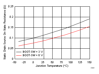
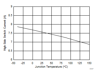
| VDD = 12 V |
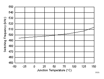
| R(RT) = 200 kΩ | VDD = 12 V |
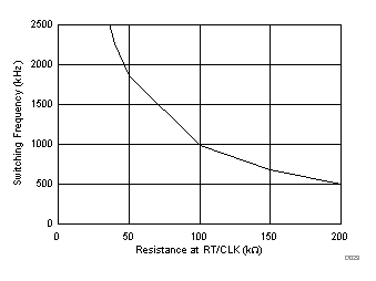
High-Frequency Range
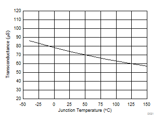
| VDD = 12 V |
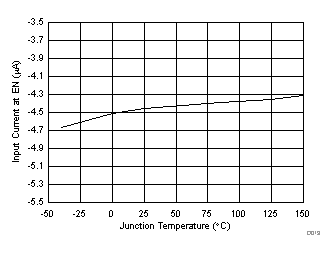
| VDD = 12 V | V(EN) = Threshold + 50 mV |
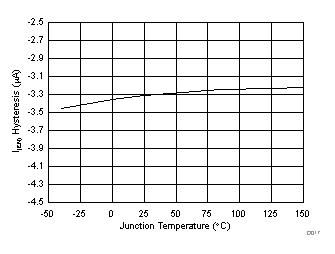
| VDD = 12 V |
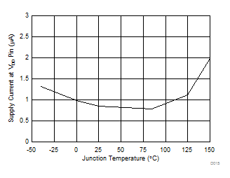
| VDD = 12 V |
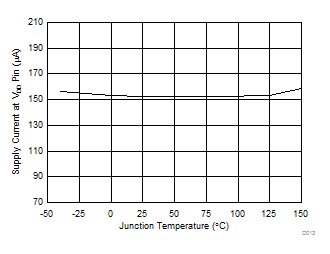
| VDD = 12 V |
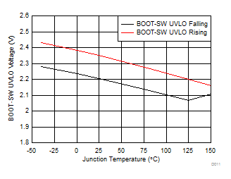
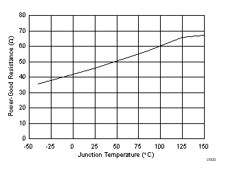
| VDD = 12 V |
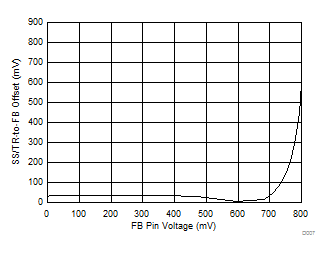
| VDD = 12 V | TJ = 25ºC |
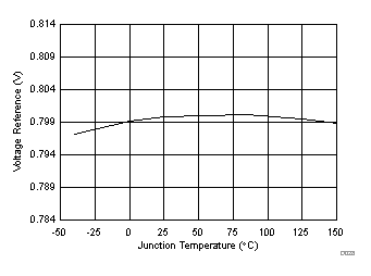
| VDD = 12 V |
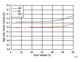
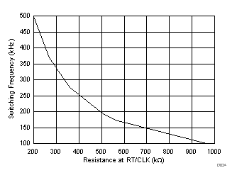
Low-Frequency Range
| VDD = 12 V |
| VDD = 12 V |
| VDD = 12 V | V(EN) = Threshold – 50 mV |
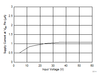
| TJ = 25ºC |
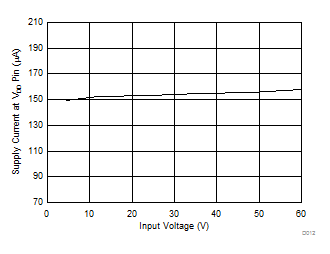
| TJ = 25ºC |
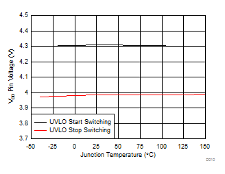
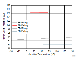
| VDD = 12 V |
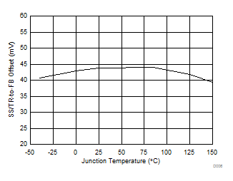
| VDD = 12 V | V(FB) = 0.4 V |
