ZHCSBY9G July 2013 – June 2021 TPS54561
PRODUCTION DATA
- 1 特性
- 2 应用
- 3 说明
- 4 Revision History
- 5 Pin Configuration and Functions
- 6 Specifications
-
7 Detailed Description
- 7.1 Overview
- 7.2 Functional Block Diagram
- 7.3
Feature Description
- 7.3.1 Fixed Frequency PWM Control
- 7.3.2 Slope Compensation Output Current
- 7.3.3 Pulse Skip Eco-mode
- 7.3.4 Low Dropout Operation and Bootstrap Voltage (BOOT)
- 7.3.5 Error Amplifier
- 7.3.6 Adjusting the Output Voltage
- 7.3.7 Enable and Adjusting Undervoltage Lockout
- 7.3.8 Soft Start/Tracking Pin (SS/TR)
- 7.3.9 Sequencing
- 7.3.10 Constant Switching Frequency and Timing Resistor (RT/CLK) Pin)
- 7.3.11 Maximum Switching Frequency
- 7.3.12 Synchronization to RT/CLK Pin
- 7.3.13 Accurate Current Limit Operation
- 7.3.14 Power Good (PWRGD Pin)
- 7.3.15 Overvoltage Protection
- 7.3.16 Thermal Shutdown
- 7.3.17 Small Signal Model for Loop Response
- 7.3.18 Simple Small Signal Model for Peak Current Mode Control
- 7.3.19 Small Signal Model for Frequency Compensation
- 7.4 Device Functional Modes
-
8 Application and Implementation
- 8.1 Application Information
- 8.2
Typical Applications
- 8.2.1
Buck Converter for 7-V to 60-V Input to 5-V at 5-A Output
- 8.2.1.1 Design Requirements
- 8.2.1.2
Detailed Design Procedure
- 8.2.1.2.1 Custom Design with WEBENCH® Tools
- 8.2.1.2.2 Selecting the Switching Frequency
- 8.2.1.2.3 Output Inductor Selection (LO)
- 8.2.1.2.4 Output Capacitor
- 8.2.1.2.5 Catch Diode
- 8.2.1.2.6 Input Capacitor
- 8.2.1.2.7 Slow Start Capacitor
- 8.2.1.2.8 Bootstrap Capacitor Selection
- 8.2.1.2.9 Undervoltage Lockout Set Point
- 8.2.1.2.10 Output Voltage and Feedback Resistors Selection
- 8.2.1.2.11 Compensation
- 8.2.1.2.12 Power Dissipation Estimate
- 8.2.1.2.13 Safe Operating Area
- 8.2.1.2.14 Discontinuous Conduction Mode and Eco-mode Boundary
- 8.2.1.3 Application Curves
- 8.2.2 Inverting Buck-Boost Topology for Positive Input to Negative Output
- 8.2.3 Split-Rail Topology for Positive Input to Negative and Positive Output
- 8.2.1
Buck Converter for 7-V to 60-V Input to 5-V at 5-A Output
- 9 Power Supply Recommendations
- 10Layout
- 11Device and Documentation Support
- 12Mechanical, Packaging, and Orderable Information
7.3.12 Synchronization to RT/CLK Pin
The RT/CLK pin can receive a frequency synchronization signal from an external system clock. To implement this synchronization feature connect a square wave to the RT/CLK pin through either circuit network shown in Figure 7-12. The square wave applied to the RT/CLK pin must switch lower than 0.5 V and higher than 2 V and have a pulse width greater than 15 ns. The synchronization frequency range is 160 kHz to 2300 kHz. The rising edge of the SW will be synchronized to the falling edge of RT/CLK pin signal. The external synchronization circuit should be designed such that the default frequency set resistor is connected from the RT/CLK pin to ground when the synchronization signal is off. When using a low impedance signal source, the frequency set resistor is connected in parallel with an ac coupling capacitor to a termination resistor (that is, 50 Ω) as shown in Figure 7-12. The two resistors in series provide the default frequency setting resistance when the signal source is turned off. The sum of the resistance should set the switching frequency close to the external CLK frequency. AC coupling the synchronization signal through a 10-pF ceramic capacitor to RT/CLK pin is recommended.
The first time the RT/CLK is pulled above the PLL threshold the TPS54561 switches from the RT resistor free-running frequency mode to the PLL synchronized mode. The internal 0.5 V voltage source is removed and the RT/CLK pin becomes high impedance as the PLL starts to lock onto the external signal. The switching frequency can be higher or lower than the frequency set with the RT/CLK resistor. The device transitions from the resistor mode to the PLL mode and locks onto the external clock frequency within 78 microseconds. During the transition from the PLL mode to the resistor programmed mode, the switching frequency will fall to 150 kHz and then increase or decrease to the resistor programmed frequency when the 0.5-V bias voltage is reapplied to the RT/CLK resistor.
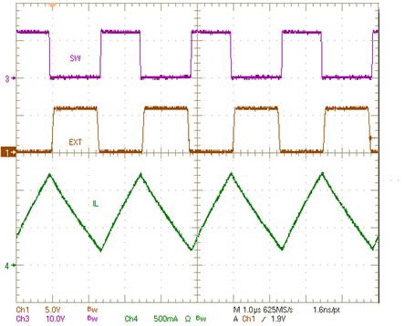
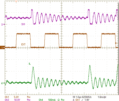
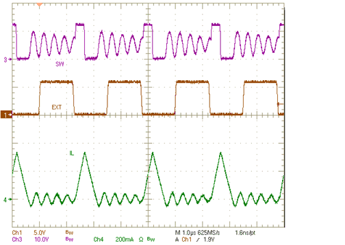
The switching frequency is divided by 8, 4, 2, and 1 as the FB pin voltage ramps from 0 to 0.8 V. The device implements a digital frequency foldback to enable synchronizing to an external clock during normal start-up and fault conditions. Figure 7-13, Figure 7-14, and Figure 7-15 show the device synchronized to an external system clock in continuous conduction mode (CCM), discontinuous conduction (DCM), and pulse skip mode (Eco-Mode).
 Figure 7-12 Synchronizing to a System Clock
 Figure 7-13 Plot
of Synchronizing in CCM
 Figure 7-15 Plot
of Synchronizing in Eco-mode
 Figure 7-14 Plot of Synchronizing in DCM