ZHCS984B June   2012  – May 2019 TPS54678

PRODUCTION DATA.  

  1. 特性
  2. 应用
  3. 说明
    1.     Device Images
      1.      简化原理图
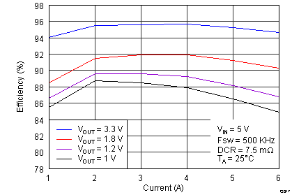
      2.      效率与输出电流间的关系
  4. 修订历史记录
  5. Pin Configuration and Functions
    1.     Pin Functions
  6. Specifications
    1. 6.1 Absolute Maximum Ratings
    2. 6.2 ESD Ratings
    3. 6.3 Recommended Operating Conditions
    4. 6.4 Thermal Information
    5. 6.5 Electrical Characteristics
    6. 6.6 Typical Characteristics
  7. Detailed Description
    1. 7.1 Overview
    2. 7.2 Functional Block Diagram
    3. 7.3 Feature Description
      1. 7.3.1  Fixed Frequency PWM Control
      2. 7.3.2  Slope Compensation and Output Current
      3. 7.3.3  Bootstrap Voltage (Boot) and Low Dropout Operation
      4. 7.3.4  Error Amplifier
      5. 7.3.5  Voltage Reference
      6. 7.3.6  Adjusting the Output Voltage
      7. 7.3.7  Enable and Adjusting Undervoltage Lockout
      8. 7.3.8  Soft-Start Pin
      9. 7.3.9  Sequencing
      10. 7.3.10 Constant Switching Frequency and Timing Resistor (RT/CLK Pin)
      11. 7.3.11 Overcurrent Protection
        1. 7.3.11.1 High-Side Overcurrent Protection
        2. 7.3.11.2 Low-Side Overcurrent Protection
      12. 7.3.12 Safe Start-Up into Prebiased Outputs
      13. 7.3.13 Synchronize Using the RT/CLK Pin
      14. 7.3.14 Power Good (PWRGD Pin)
      15. 7.3.15 Overvoltage Transient Protection
      16. 7.3.16 Thermal Shutdown
    4. 7.4 Device Functional Modes
      1. 7.4.1 Small Signal Model for Loop Response
      2. 7.4.2 Simple Small Signal Model for Peak Current Mode Control
      3. 7.4.3 Small Signal Model for Frequency Compensation
  8. Application and Implementation
    1. 8.1 Application Information
    2. 8.2 Typical Application
      1. 8.2.1 Design Requirements
      2. 8.2.2 Detailed Design Procedure
        1. 8.2.2.1 Custom Design With WEBENCH® Tools
        2. 8.2.2.2 Step One: Select the Switching Frequency
        3. 8.2.2.3 Step Two: Select the Output Inductor
        4. 8.2.2.4 Step Three: Choose the Output Capacitor
        5. 8.2.2.5 Step Four: Select the Input Capacitor
        6. 8.2.2.6 Step Five: Choose the Soft-Start Capacitor
        7. 8.2.2.7 Step Six: Select the Bootstrap Capacitor
        8. 8.2.2.8 Step Eight: Select Output Voltage and Feedback Resistors
          1. 8.2.2.8.1 Output Voltage Limitations
        9. 8.2.2.9 Step Nine: Select Loop Compensation Components
      3. 8.2.3 Application Curves
        1. 8.2.3.1 Additional Information About Application Curves
          1. 8.2.3.1.1 Efficiency
          2. 8.2.3.1.2 Voltage Ripple Measurements
          3. 8.2.3.1.3 Start-Up and Shutdown Waveforms
          4. 8.2.3.1.4 Hiccup Mode Current Limit
  9. Power Supply Recommendations
  10. 10Layout
    1. 10.1 Layout Guidelines
    2. 10.2 Layout Example
    3. 10.3 Power Dissipation Estimate
  11. 11器件和文档支持
    1. 11.1 器件支持
      1. 11.1.1 第三方米6体育平台手机版_好二三四免责声明
      2. 11.1.2 开发支持
        1. 11.1.2.1 使用 WEBENCH® 工具创建定制设计
    2. 11.2 文档支持
      1. 11.2.1 相关文档
    3. 11.3 接收文档更新通知
    4. 11.4 社区资源
    5. 11.5 商标
    6. 11.6 静电放电警告
    7. 11.7 Glossary
  12. 12机械、封装和可订购信息

封装选项

机械数据 (封装 | 引脚)
散热焊盘机械数据 (封装 | 引脚)
订购信息

Typical Characteristics
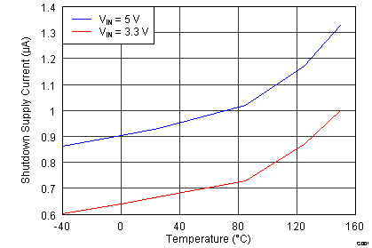
TPS54678 G001_SLVSBF3.png
Figure 1. Shutdown Supply Current vs Junction Temperature
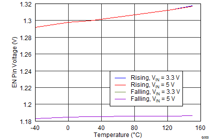
TPS54678 G003_SLVSBF3.png
Figure 3. EN Pin Voltage vs Junction Temperature
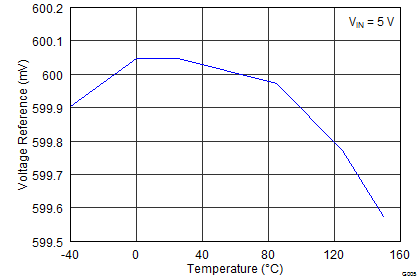
TPS54678 G005_SLVSBF3.png
Figure 5. Voltage Reference vs Junction Temperature
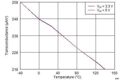
TPS54678 G007_SLVSBF3.png
Figure 7. Transconductance vs Junction Temperature
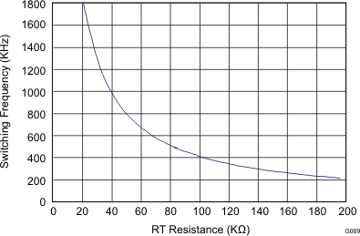
TPS54678 G009_SLVSBF3.gif
Figure 9. Switching Frequency vs RT Pin Resistance
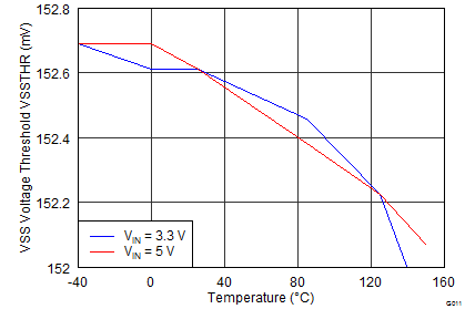
TPS54678 G011_SLVSBF3.png
Figure 11. VSS Voltage Threshold vs Junction Temperature
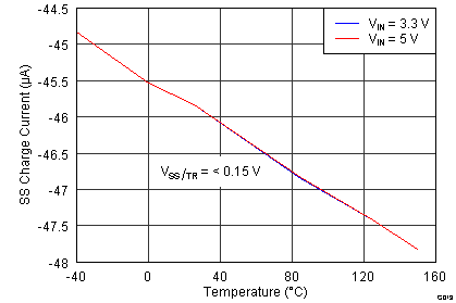
TPS54678 G013_SLVSBF3.png
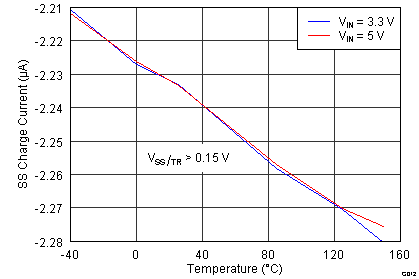
Figure 13. SS Charge Current vs Junction Temperature
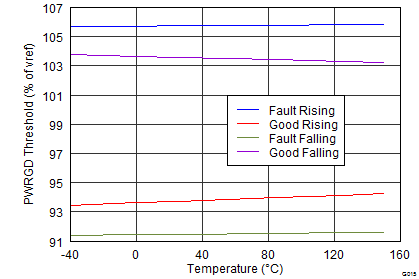
TPS54678 G015_SLVSBF3.png
Figure 15. PWRGD Threshold vs Junction Temperature
TPS54678 G017_SLVSBF3.png
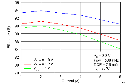
Figure 17. Efficiency vs Load Current
TPS54678 G019_SLVSBF3.png
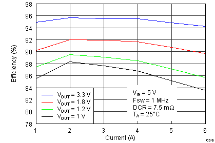
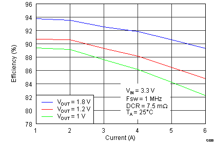
Figure 19. Efficiency vs Load Current
TPS54678 G002_SLVSBF3.png
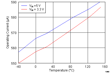
Figure 2. VIN Operating Current vs Junction Temperature
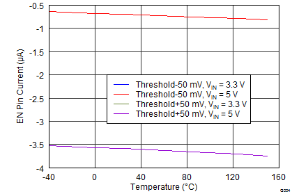
TPS54678 G004_SLVSBF3.png
Figure 4. EN Pin Current vs Junction Temperature
TPS54678 G006_SLVSBF3.png
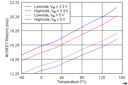
Figure 6. MOSFET Rds(on) vs Junction Temperature
TPS54678 G008_SLVSBF3.png
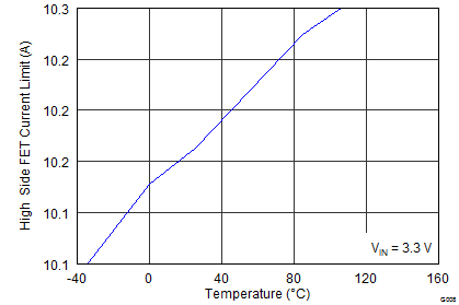
Figure 8. High-Side FET Current Limit vs Junction Temperature
TPS54678 G010_SLVSBF3.png
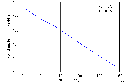
Figure 10. Switching Frequency vs Junction Temperature
TPS54678 G012_SLVSBF3.png
Figure 12. SS Charge Current vs Junction Temperature
TPS54678 G014_SLVSBF3.png
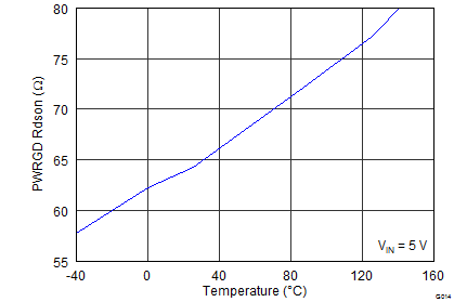
Figure 14. PWRGD Rds(on) vs Junction Temperature
TPS54678 G016_SLVSBF3.png
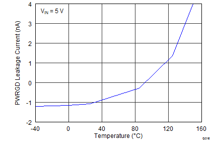
Figure 16. PWRGD Leakage Current vs Junction Temperature
TPS54678 G018_SLVSBF3.png
Figure 18. Efficiency vs Load Current
TPS54678 G020_SLVSBF3.png
Figure 20. Efficiency vs Load Current