ZHCSFG3B July 2016 – December 2016 TPS546C20A
PRODUCTION DATA.
- 1 特性
- 2 应用范围
- 3 说明
- 4 修订历史记录
- 5 Pin Configuration and Functions
- 6 Specifications
-
7 Detailed Description
- 7.1 Overview
- 7.2 Functional Block Diagram
- 7.3
Feature Description
- 7.3.1 2-Phase Application
- 7.3.2 Linear Regulators BP3 and BP6
- 7.3.3 Input Undervoltage Lockout (UVLO)
- 7.3.4 Turnon and Turnoff Delay and Sequencing
- 7.3.5 Voltage Reference
- 7.3.6 Differential Remote Sense and Compensation
- 7.3.7 Set Output Voltage and Adaptive Voltage Scaling (AVS)
- 7.3.8 Reset VOUT
- 7.3.9 Switching Frequency and Synchronization
- 7.3.10 Current Sharing
- 7.3.11 Soft-Start Time and TON_RISE Command
- 7.3.12 Prebiased Output Start-Up
- 7.3.13 Soft-Stop time and TOFF_FALL Command
- 7.3.14 Output Current Telemetry and Low-Side MOSFET Overcurrent Protection
- 7.3.15 High-Side MOSFET Short-Circuit Protection
- 7.3.16 Die Temperature Telemetry and Overtemperature Protection
- 7.3.17 Output Voltage Telemetry and Over-/Under-voltage Protection
- 7.3.18 TON_MAX Fault
- 7.3.19 Power Good (PGOOD) Indicator
- 7.3.20 Fault Protection Responses
- 7.3.21 Switching Node
- 7.3.22 PMBus General Description
- 7.3.23 PMBus Address
- 7.3.24 PMBus Connections
- 7.3.25 Auto ARA (Alert Response Address) Response
- 7.4 Device Functional Modes
- 7.5 Programming
- 7.6
Register Maps
- 7.6.1 OPERATION (01h)
- 7.6.2 ON_OFF_CONFIG (02h)
- 7.6.3 CLEAR_FAULTS (03h)
- 7.6.4 WRITE_PROTECT (10h)
- 7.6.5 STORE_DEFAULT_ALL (11h)
- 7.6.6 RESTORE_DEFAULT_ALL (12h)
- 7.6.7 STORE_USER_ALL (11h)
- 7.6.8 RESTORE_USER_ALL (12h)
- 7.6.9 CAPABILITY (19h)
- 7.6.10 SMBALERT_MASK (1Bh)
- 7.6.11 VOUT_MODE (20h)
- 7.6.12 VOUT_COMMAND (21h)
- 7.6.13 VOUT_MAX (24h)
- 7.6.14 VOUT_TRANSITION_RATE (27h)
- 7.6.15 VOUT_SCALE_LOOP (29h)
- 7.6.16 VOUT_MIN (2Bh)
- 7.6.17 VIN_ON (35h)
- 7.6.18 VIN_OFF (36h)
- 7.6.19 IOUT_CAL_OFFSET (39h)
- 7.6.20 VOUT_OV_FAULT_RESPONSE (41h)
- 7.6.21 VOUT_UV_FAULT_RESPONSE (45h)
- 7.6.22 IOUT_OC_FAULT_LIMIT (46h)
- 7.6.23 IOUT_OC_FAULT_RESPONSE (47h)
- 7.6.24 IOUT_OC_WARN_LIMIT (4Ah)
- 7.6.25 OT_FAULT_LIMIT (4Fh)
- 7.6.26 OT_FAULT_RESPONSE (50h)
- 7.6.27 OT_WARN_LIMIT (51h)
- 7.6.28 TON_DELAY (60h)
- 7.6.29 TON_RISE (61h)
- 7.6.30 TON_MAX_FAULT_LIMIT (62h)
- 7.6.31 TON_MAX_FAULT_RESPONSE (63h)
- 7.6.32 TOFF_DELAY (64h)
- 7.6.33 TOFF_FALL (65h)
- 7.6.34 STATUS_BYTE (78h)
- 7.6.35 STATUS_WORD (79h)
- 7.6.36 STATUS_VOUT (7Ah)
- 7.6.37 STATUS_IOUT (7Bh)
- 7.6.38 STATUS_INPUT (7Ch)
- 7.6.39 STATUS_TEMPERATURE (7Dh)
- 7.6.40 STATUS_CML (7Eh)
- 7.6.41 STATUS_MFR_SPECIFIC (80h)
- 7.6.42 READ_VOUT (8Bh)
- 7.6.43 READ_IOUT (8Ch)
- 7.6.44 READ_TEMPERATURE_1 (8Dh)
- 7.6.45 PMBUS_REVISION (98h)
- 7.6.46 IC_DEVICE_ID (ADh)
- 7.6.47 IC_DEVICE_REV (AEh)
- 7.6.48 MFR_SPECIFIC_00 (D0h)
- 7.6.49 VREF_TRIM (MFR_SPECIFIC_04) (D4h)
- 7.6.50 STEP_VREF_MARGIN_HIGH (MFR_SPECIFIC_05) (D5h)
- 7.6.51 STEP_VREF_MARGIN_LOW (MFR_SPECIFIC_06) (D6h)
- 7.6.52 PCT_OV_UV_WRN_FLT_LIMITS (MFR_SPECIFIC_07) (D7h)
- 7.6.53
OPTIONS (MFR_SPECIFIC_21) (E5h)
- 7.6.53.1 DIS_NEGILIM Bit
- 7.6.53.2 EN_RESET_B Bit
- 7.6.53.3 EN_ADC_CNTL Bit
- 7.6.53.4 VSM Bit
- 7.6.53.5 DLO Bit
- 7.6.53.6 AVG_PROG[1:0] Bits
- 7.6.53.7 EN_AUTO_ARA Bit
- 7.6.53.8 READ_VOUT_RANGE[1:0] Bits
- 7.6.53.9 EN_DRV_IV_VSEL Bit
- 7.6.53.10 RST_VOUT_oSD Bit
- 7.6.53.11 DIS_VSEL Bit
- 7.6.53.12 RSMLO_VAL Bit
- 7.6.53.13 RSMHI_VAL Bit
- 7.6.54 MISC_CONFIG_OPTIONS (MFR_SPECIFIC_32) (F0h)
-
8 Applications and Implementation
- 8.1 Application Information
- 8.2
Typical Application
- 8.2.1
4.5-V to 18-V Input, 1-V Typical Output, 35-A Converter
- 8.2.1.1 Design Requirements
- 8.2.1.2
Detailed Design Procedure
- 8.2.1.2.1 Switching Frequency Selection
- 8.2.1.2.2 Inductor Selection
- 8.2.1.2.3 Output Capacitor Selection
- 8.2.1.2.4 Output Voltage Deviation During Load Transient
- 8.2.1.2.5 Output Voltage Ripple
- 8.2.1.2.6 Input Capacitor Selection
- 8.2.1.2.7 AVIN, BP6, BP3 Bypass Capacitor
- 8.2.1.2.8 Bootstrap Capacitor Selection
- 8.2.1.2.9 R-C Snubber
- 8.2.1.2.10 Output Voltage Setting and Frequency Compensation Selection
- 8.2.1.2.11 Key PMBus Parameter Selection
- 8.2.1.2.12 Enable, UVLO
- 8.2.1.2.13 Soft-Start Time
- 8.2.1.2.14 Overcurrent Threshold and Response
- 8.2.1.3 Application Curves
- 8.2.1
4.5-V to 18-V Input, 1-V Typical Output, 35-A Converter
- 9 Power Supply Recommendations
- 10Layout
- 11器件和文档支持
- 12机械、封装和可订购信息
10 Layout
10.1 Layout Guidelines
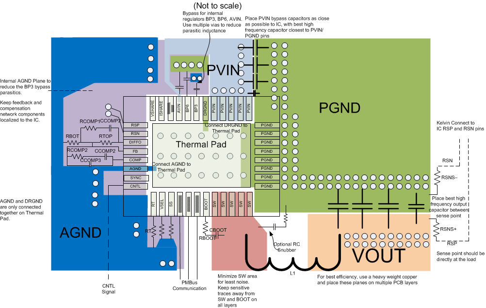
Layout is critical for good power-supply design. Figure 52 shows the recommended PCB-layout configuration. A list of PCB layout considerations using these devices is listed as follows:
- As with any switching regulator, several power or signal paths exist that conduct fast switching voltages or currents. Minimize the loop area formed by these paths and their bypass connections.
- Bypass the PVIN pins to PGND with a low-impedance path. The input bypass capacitors of the power-stage should be placed as close as physically possible to the PVIN and PGND pins. Additionally, a high-frequency bypass capacitor in a 0402 package on the PVIN pins can help reduce switching spikes. This capacitor which can be placed on the other side of the PCB directly underneath the device to keep a minimum loop.
- The BP6 bypass capacitor carries a large switching current for the gate driver. Bypassing the BP6 pin to PGND with a low-impedance path is very critical to the stable operation of the devices. Place the BP6 high-frequency bypass capacitors as close as possible to the device pins, with a minimum return loop back to ground.
- The AVIN and BP3 pins also require good local bypassing. Place bypass capacitors as close as possible to the device pins, with a minimum return loop back to ground. This return loop should be kept away from fast switching voltages, the main current path, and the BP6 current path. Poor bypassing on the AVIN and BP3 pins can degrade the performance of the device.
- Keep signal components local to the device, and place them as close as possible to the pins to which they are connected. These components include the feedback resistors and the RT resistor. These components should also be kept away from fast switching voltage and current paths. Those components can be terminated to AGND with a minimum return loop or bypassed to the copper area of a separate low-impedance analog ground (AGND) that is isolated from fast switching voltages and current paths and has single connection to PGND on the thermal pad through the AGND pin. For placement recommendations, see Figure 52.
- The PGND pin (pin 26) must be directly connected to the thermal pad of the device on the PCB, with a low-noise, low-impedance path to ensure accurate current monitoring.
- Minimize the SW copper area for best noise performance. Route sensitive traces away from the SW and BOOT pins as these nets contain fast switching voltages and lend easily to capacitive coupling.
- Snubber component placement is critical for effective ringing reduction. These components should be on the same layer as the devices, and be kept as close as possible to the SW and PGND copper areas.
- The PVIN and AVIN pins must be the same potential for accurate short circuit protection, but high-frequency switching noise on the AVIN pin can degrade performance. The AVIN pin should be connected to PVIN through a trace from the input copper area. Optionally form a small low-pass R-C between the PVIN and AVIN pins, with the AVIN bypass capacitor (1 µF) and a 0-2 Ω resistor between the PVIN and AVIN pins. See Figure 52 for placement recommendations.
- Route the RSP and RSN lines from the output capacitor bank at the load back to the device pins as a tightly coupled differential pair. These traces must be kept away from switching or noisy areas which can add differential-mode noise.
- Use caution when routing of the SYNC, VSHARE and ISHARE traces for 2-phase configurations. The SYNC trace carries a rail-to-rail signal and should be routed away from sensitive analog signals, including the VSHARE, ISHARE, RT, and FB signals. The VSHARE and ISHARE traces should also be kept away from fast switching voltages or currents formed by the PVIN, AVIN, SW, BOOT, BP6 pins.
10.2 Layout Example
 Figure 52. PCB Layout Recommendation
10.3 Mounting and Thermal Profile Recommendation
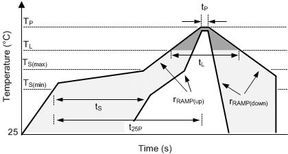
Proper mounting technique adequately covers the exposed thermal pad with solder. Excessive heat during the reflow process can affect electrical performance. Figure 53 shows the recommended reflow-oven thermal profile. Proper post-assembly cleaning is also critical to device performance. Refer to QFN/SON PCB Attachment (SLUA271) for more information.
 Figure 53. Recommended Reflow-Oven Thermal Profile
Table 17. Recommended Thermal Profile Parameters
| PARAMETER | MIN | TYP | MAX | UNIT | |
|---|---|---|---|---|---|
| RAMP UP AND RAMP DOWN | |||||
| rRAMP(up) | Average ramp-up rate, TS(max) to TP | 3 | °C/s | ||
| rRAMP(down) | Average ramp-down rate, TP to TS(max) | 6 | °C/s | ||
| PRE-HEAT | |||||
| TS | Preheat temperature | 150 | 200 | °C | |
| tS | Preheat time, TS(min) to TS(max) | 60 | 180 | s | |
| REFLOW | |||||
| TL | Liquidus temperature | 217 | °C | ||
| TP | Peak temperature | 260 | °C | ||
| tL | Time maintained above liquidus temperature, TL | 60 | 150 | s | |
| tP | Time maintained within 5°C of peak temperature, TP | 20 | 40 | s | |
| t25P | Total time from 25°C to peak temperature, TP | 480 | s | ||