ZHCSFG3B July 2016 – December 2016 TPS546C20A
PRODUCTION DATA.
- 1 特性
- 2 应用范围
- 3 说明
- 4 修订历史记录
- 5 Pin Configuration and Functions
- 6 Specifications
-
7 Detailed Description
- 7.1 Overview
- 7.2 Functional Block Diagram
- 7.3
Feature Description
- 7.3.1 2-Phase Application
- 7.3.2 Linear Regulators BP3 and BP6
- 7.3.3 Input Undervoltage Lockout (UVLO)
- 7.3.4 Turnon and Turnoff Delay and Sequencing
- 7.3.5 Voltage Reference
- 7.3.6 Differential Remote Sense and Compensation
- 7.3.7 Set Output Voltage and Adaptive Voltage Scaling (AVS)
- 7.3.8 Reset VOUT
- 7.3.9 Switching Frequency and Synchronization
- 7.3.10 Current Sharing
- 7.3.11 Soft-Start Time and TON_RISE Command
- 7.3.12 Prebiased Output Start-Up
- 7.3.13 Soft-Stop time and TOFF_FALL Command
- 7.3.14 Output Current Telemetry and Low-Side MOSFET Overcurrent Protection
- 7.3.15 High-Side MOSFET Short-Circuit Protection
- 7.3.16 Die Temperature Telemetry and Overtemperature Protection
- 7.3.17 Output Voltage Telemetry and Over-/Under-voltage Protection
- 7.3.18 TON_MAX Fault
- 7.3.19 Power Good (PGOOD) Indicator
- 7.3.20 Fault Protection Responses
- 7.3.21 Switching Node
- 7.3.22 PMBus General Description
- 7.3.23 PMBus Address
- 7.3.24 PMBus Connections
- 7.3.25 Auto ARA (Alert Response Address) Response
- 7.4 Device Functional Modes
- 7.5 Programming
- 7.6
Register Maps
- 7.6.1 OPERATION (01h)
- 7.6.2 ON_OFF_CONFIG (02h)
- 7.6.3 CLEAR_FAULTS (03h)
- 7.6.4 WRITE_PROTECT (10h)
- 7.6.5 STORE_DEFAULT_ALL (11h)
- 7.6.6 RESTORE_DEFAULT_ALL (12h)
- 7.6.7 STORE_USER_ALL (11h)
- 7.6.8 RESTORE_USER_ALL (12h)
- 7.6.9 CAPABILITY (19h)
- 7.6.10 SMBALERT_MASK (1Bh)
- 7.6.11 VOUT_MODE (20h)
- 7.6.12 VOUT_COMMAND (21h)
- 7.6.13 VOUT_MAX (24h)
- 7.6.14 VOUT_TRANSITION_RATE (27h)
- 7.6.15 VOUT_SCALE_LOOP (29h)
- 7.6.16 VOUT_MIN (2Bh)
- 7.6.17 VIN_ON (35h)
- 7.6.18 VIN_OFF (36h)
- 7.6.19 IOUT_CAL_OFFSET (39h)
- 7.6.20 VOUT_OV_FAULT_RESPONSE (41h)
- 7.6.21 VOUT_UV_FAULT_RESPONSE (45h)
- 7.6.22 IOUT_OC_FAULT_LIMIT (46h)
- 7.6.23 IOUT_OC_FAULT_RESPONSE (47h)
- 7.6.24 IOUT_OC_WARN_LIMIT (4Ah)
- 7.6.25 OT_FAULT_LIMIT (4Fh)
- 7.6.26 OT_FAULT_RESPONSE (50h)
- 7.6.27 OT_WARN_LIMIT (51h)
- 7.6.28 TON_DELAY (60h)
- 7.6.29 TON_RISE (61h)
- 7.6.30 TON_MAX_FAULT_LIMIT (62h)
- 7.6.31 TON_MAX_FAULT_RESPONSE (63h)
- 7.6.32 TOFF_DELAY (64h)
- 7.6.33 TOFF_FALL (65h)
- 7.6.34 STATUS_BYTE (78h)
- 7.6.35 STATUS_WORD (79h)
- 7.6.36 STATUS_VOUT (7Ah)
- 7.6.37 STATUS_IOUT (7Bh)
- 7.6.38 STATUS_INPUT (7Ch)
- 7.6.39 STATUS_TEMPERATURE (7Dh)
- 7.6.40 STATUS_CML (7Eh)
- 7.6.41 STATUS_MFR_SPECIFIC (80h)
- 7.6.42 READ_VOUT (8Bh)
- 7.6.43 READ_IOUT (8Ch)
- 7.6.44 READ_TEMPERATURE_1 (8Dh)
- 7.6.45 PMBUS_REVISION (98h)
- 7.6.46 IC_DEVICE_ID (ADh)
- 7.6.47 IC_DEVICE_REV (AEh)
- 7.6.48 MFR_SPECIFIC_00 (D0h)
- 7.6.49 VREF_TRIM (MFR_SPECIFIC_04) (D4h)
- 7.6.50 STEP_VREF_MARGIN_HIGH (MFR_SPECIFIC_05) (D5h)
- 7.6.51 STEP_VREF_MARGIN_LOW (MFR_SPECIFIC_06) (D6h)
- 7.6.52 PCT_OV_UV_WRN_FLT_LIMITS (MFR_SPECIFIC_07) (D7h)
- 7.6.53
OPTIONS (MFR_SPECIFIC_21) (E5h)
- 7.6.53.1 DIS_NEGILIM Bit
- 7.6.53.2 EN_RESET_B Bit
- 7.6.53.3 EN_ADC_CNTL Bit
- 7.6.53.4 VSM Bit
- 7.6.53.5 DLO Bit
- 7.6.53.6 AVG_PROG[1:0] Bits
- 7.6.53.7 EN_AUTO_ARA Bit
- 7.6.53.8 READ_VOUT_RANGE[1:0] Bits
- 7.6.53.9 EN_DRV_IV_VSEL Bit
- 7.6.53.10 RST_VOUT_oSD Bit
- 7.6.53.11 DIS_VSEL Bit
- 7.6.53.12 RSMLO_VAL Bit
- 7.6.53.13 RSMHI_VAL Bit
- 7.6.54 MISC_CONFIG_OPTIONS (MFR_SPECIFIC_32) (F0h)
-
8 Applications and Implementation
- 8.1 Application Information
- 8.2
Typical Application
- 8.2.1
4.5-V to 18-V Input, 1-V Typical Output, 35-A Converter
- 8.2.1.1 Design Requirements
- 8.2.1.2
Detailed Design Procedure
- 8.2.1.2.1 Switching Frequency Selection
- 8.2.1.2.2 Inductor Selection
- 8.2.1.2.3 Output Capacitor Selection
- 8.2.1.2.4 Output Voltage Deviation During Load Transient
- 8.2.1.2.5 Output Voltage Ripple
- 8.2.1.2.6 Input Capacitor Selection
- 8.2.1.2.7 AVIN, BP6, BP3 Bypass Capacitor
- 8.2.1.2.8 Bootstrap Capacitor Selection
- 8.2.1.2.9 R-C Snubber
- 8.2.1.2.10 Output Voltage Setting and Frequency Compensation Selection
- 8.2.1.2.11 Key PMBus Parameter Selection
- 8.2.1.2.12 Enable, UVLO
- 8.2.1.2.13 Soft-Start Time
- 8.2.1.2.14 Overcurrent Threshold and Response
- 8.2.1.3 Application Curves
- 8.2.1
4.5-V to 18-V Input, 1-V Typical Output, 35-A Converter
- 9 Power Supply Recommendations
- 10Layout
- 11器件和文档支持
- 12机械、封装和可订购信息
6 Specifications
6.1 Absolute Maximum Ratings
over operating free-air temperature range (unless otherwise noted) (1)| MIN | MAX | UNIT | ||
|---|---|---|---|---|
| Input voltage | PVIN, AVIN | –0.3 | 18 | V |
| PVIN, AVIN< 2 ms transient | –0.3 | 19 | ||
| PVIN - SW (PVIN to SW differential) | –0.3 | 25 | ||
| PVIN - SW (PVIN to SW differential, < 10-ns transient because of SW ringing) | –5 | 25 | ||
| BOOT | –0.3 | 37 | ||
| BOOT – SW (BOOT to SW differential) | –0.3 | 7 | ||
| PMB_CLK, PMB_DATA | –0.3 | 5.5 | ||
| VSEL, SS | –0.3 | 3.6 | ||
| SYNC, RESET/PGD, CNTL, RSP, RSN, RT, ISHARE, FB | –0.3 | 7 | ||
| Output voltage | SW | –1 | 25 | V |
| SW < 100 ns transient | –5 | 25 | ||
| BP6, COMP, DIFFO, VSHARE | –0.3 | 7 | ||
| SMB_ALRT | –0.3 | 5.5 | ||
| BP3 | –0.3 | 3.6 | ||
| Operating junction temperature, TJ | –40 | 150 | °C | |
| Storage temperature, Tstg | –55 | 150 | °C | |
(1) Stresses beyond those listed under Absolute Maximum Ratings may cause permanent damage to the device. These are stress ratings only, which do not imply functional operation of the device at these or any other conditions beyond those indicated under Recommended Operating Conditions. Exposure to absolute-maximum-rated conditions for extended periods may affect device reliability.
6.2 ESD Ratings
| VALUE | UNIT | |||
|---|---|---|---|---|
| V(ESD) | Electrostatic discharge | Human-body model (HBM), per ANSI/ESDA/JEDEC JS–001(1) | ±2000 | V |
| Charged-device model (CDM), per JEDEC specification JESD22-C101(2) | ±1500 | |||
(1) JEDEC document JEP155 states that 500-V HBM allows safe manufacturing with a standard ESD control process.
(2) JEDEC document JEP157 states that 250-V CDM allows safe manufacturing with a standard ESD control process.
6.3 Recommended Operating Conditions
over operating free-air temperature range (unless otherwise noted)| MIN | NOM | MAX | UNIT | ||
|---|---|---|---|---|---|
| VAVIN | Controller input voltage | 4.5 | 12 | 18 | V |
| VPVIN | Power stage input voltage | 4.5 | 12 | 18 | V |
| TJ | Junction temperature | –40 | 125 | °C | |
6.4 Thermal Information
| THERMAL METRIC(1) | TPS546C20A | UNIT | |
|---|---|---|---|
| RVF (PQFN) | |||
| 40 PINS | |||
| RθJA | Junction-to-ambient thermal resistance | 28.5 | °C/W |
| RθJC(top) | Junction-to-case (top) thermal resistance | 18 | °C/W |
| RθJB | Junction-to-board thermal resistance | 3.8 | °C/W |
| ψJT | Junction-to-top characterization parameter | 1 | °C/W |
| ψJB | Junction-to-board characterization parameter | 3.8 | °C/W |
| RθJC(bot) | Junction-to-case (bottom) thermal resistance | 0.7 | °C/W |
(1) For more information about traditional and new thermal metrics, see the Semiconductor and IC Package Thermal Metrics application report (SPRA953).
6.5 Electrical Characteristics
TJ = –40°C to 125°C, VPVIN = VAVIN= 12 V, RRT = 40.2 kΩ; zero power dissipation (unless otherwise noted)| PARAMETER | TEST CONDITIONS | MIN | TYP | MAX | UNIT | ||
|---|---|---|---|---|---|---|---|
| INPUT SUPPLY | |||||||
| VAVIN | Input supply voltage range | 4.5 | 18 | V | |||
| VPVIN | Power stage voltage range | 4.5 | 18 | ||||
| IAVIN | Input Operating Current | Not switching | 7.7 | 12 | mA | ||
| UVLO | |||||||
| VIN_ON | Input turnon voltage | Factory default setting | 4.5 | V | |||
| Programmable range, 15 different settings | 4.25 | 7.75 | |||||
| Accuracy | –5% | 5% | |||||
| VIN_OFF | Input turnoff voltage | Factory default setting | 4 | V | |||
| Programmable range, 15 different settings | 4 | 7.5 | |||||
| Accuracy | –5% | 5% | |||||
| ERROR AMPLIFIER AND FEEDBACK VOLTAGE | |||||||
| VFB | Feedback pin voltage | Default setting | 600 | mV | |||
| Setpoint range(1) | 0.35 | 1.65 | V | ||||
| Setpoint resolution(1) | 2-9 | V | |||||
| VFB(ACC) | Feedback pin voltage accuracy | VFB = 600 mV, 0°C ≤ TJ ≤ 85°C(2) | –0.5% | 0.5% | % | ||
| VFB = 600 mV, -40°C ≤ TJ ≤ 125°C(2) | –1% | 1% | |||||
| VFB = 1650 mV, -40°C ≤ TJ ≤ 125°C(2) | –1% | 1% | |||||
| VFB = 350 mV, -40°C ≤ TJ ≤ 125°C(2) | –1.5% | 1.5% | |||||
| AOL | Open-loop gain(1) | 80 | dB | ||||
| GBWP | Gain bandwidth product(1) | 15 | MHz | ||||
| IFB | FB pin input bias current | VFB = 0.6 V | -75 | 75 | nA | ||
| ICOMP | Sourcing | VFB = 0 V | 1 | mA | |||
| Sinking | VFB = 1.2 V | 1 | mA | ||||
| OSCILLATOR | |||||||
| fSW | Adjustment range(2) | 200 | 1000 | kHz | |||
| Switching frequency(2) | RRT = 40.2 kΩ | 450 | 500 | 550 | kHz | ||
| VRMP | Ramp peak-to-peak(1) | VAVIN/6.5 | V | ||||
| VVLY | Valley voltage(1) | 1.23 | V | ||||
| SYNCHRONIZATION | |||||||
| VIH(sync) | High-level input voltage | 2.2 | V | ||||
| VIL(sync) | Low-level input voltage | 0.80 | V | ||||
| Tpw(sync) | Sync input iminimum pulse width | Fsw = 160kHz to 1.2MHz | 200 | ns | |||
| TMdelay(sync) | Delay from the rising edge of SYNC input to the SW rising edge of the loop master device | 515 | ns | ||||
| TS delay(sync) | Delay from the falling edge of SYNC input to the SW rising edge of the loop slave device | 515 | ns | ||||
| fSYNC | Synchronization frequency | 160 | 1200 | kHz | |||
| ΔfSYNC | SYNC pin frequency range from free running frequency(1) | –20% | 20% | ||||
| RESET | |||||||
| VIH(reset) | High-level input voltage(1) | 1.35 | V | ||||
| VIL(reset) | Low-level input voltage | 0.8 | |||||
| Tpw(reset) | Minimum RESET_B pulse width | 200 | ns | ||||
| BP6 REGULATOR | |||||||
| VBP6 | Regulator output voltage | IBP6 = 10 mA | 5.85 | 6.4 | 6.95 | V | |
| VBP6(do) | Regulator dropout voltage | VAVIN – VBP6, VAVIN = 4.5 V, IBP6 = 25 mA | 100 | 200 | 400 | mV | |
| IBP6SC | Regulator short-circuit current(1) | VAVIN = 12 V | 150 | mA | |||
| VBP6UV | Regulator UVLO voltage(1) | 3.73 | V | ||||
| VBP6UV(hyst) | Regulator UVLO voltage hysteresis(1) | 270 | mV | ||||
| BOOTSTRAP | |||||||
| VBOOT(drop) | Bootstrap voltage drop | IBOOT = 5 mA | 150 | mV | |||
| BP3 REGULATOR | |||||||
| VBP3 | 3-V regulator output voltage | VAVIN ≥ 4.5 V, IBP3 = 5 mA | 3 | 3.2 | 3.4 | V | |
| IBP3SC | 3-V regulator short-circuit current(1) | 18 | 35 | mA | |||
| PWM | |||||||
| TON(min) | Minimum controllable pulse width(1) | 100 | ns | ||||
| TOFF(min) | Minimum off-time(1) | 515 | 550 | ns | |||
| SOFT START | |||||||
| TON_RISE | Soft-start time | Factory default setting | 3 | ms | |||
| Programmable range, 16 discrete settings(1) (3) | 0 | 100 | |||||
| Accuracy, TON_RISE = 3 ms, VOUT_COMMAND = 0.95 V | –10% | 10% | |||||
| TON_MAX_FAULT_LIMIT | Upper limit on the time to power up the output | Factory default setting(4) | 0 | ms | |||
| Programmable range, 16 discrete settings(1) (4) | 0 | 100 | |||||
| Accuracy(1) | –10% | 10% | |||||
| TON_DELAY | Turn-on delay | Factory default setting | 0 | ms | |||
| Programmable range, 16 discrete settings(1) | 0 | 100 | |||||
| Accuracy(1) | –10% | 10% | |||||
| SOFT STOP | |||||||
| TOFF_FALL | Soft-stop time | Factory default setting(5) | 0 | ms | |||
| Programmable range, 16 discrete settings(1) (5) | 0 | 100 | |||||
| Accuracy, TOFF_FALL = 1 ms, VOUT_COMMAND = 0.95V | –10% | 10% | |||||
| TOFF_DELAY | Turn-off delay | Factory default setting | 0 | ms | |||
| Programmable range, 16 discrete settings(1) | 0 | 100 | |||||
| Accuracy(1) | –10% | 10% | |||||
| REMOTE SENSE AMPLIFIER | |||||||
| VDIFFO(ERROR) | Error Voltage from DIFFO to (RSP – RSN) | (VRSP – VRSN) = 0.6 V | –4 | 4 | mV | ||
| (VRSP – VRSN) = 1.2 V | –5 | 5 | |||||
| (VRSP – VRSN) = 3 V | –15 | 15 | |||||
| BW | Closed-loop bandwidth(1) | 2 | MHz | ||||
| VDIFFO(max) | Maximum DIFFO output voltage | VBP6–0.2 | V | ||||
| IDIFFO | DIFFO sourcing current | 1 | mA | ||||
| DIFFO sinking current | 1 | mA | |||||
| POWER STAGE | |||||||
| RHS | High-side power device on-resistance | VBOOT - VSW = 4.5 V, TJ = 25°C | 3.5 | mΩ | |||
| VBOOT - VSW = 6.3V, TJ = 25°C | 3.2 | mΩ | |||||
| RLS | Low-side power device on-resistance | VAVIN = 4.5 V, TJ = 25°C | 1.5 | mΩ | |||
| VAVIN ≥ 12 V, TJ = 25°C | 1.4 | mΩ | |||||
| TDEAD(LtoH) | Power stage driver dead-time from Low-side off to High-side on | VAVIN ≥ 12 V, TJ = 25°C(1) | 15 | ns | |||
| TDEAD(HtoL) | Power stage driver dead-time from High-side off to Low-side on | VAVIN ≥ 12 V, TJ = 25°C(1) | 15 | ns | |||
| CURRENT SHARING | |||||||
| ISHARE(acc) | Output current sharing accuracy of two devices defined as the ratio of the current difference between two devices to the total current | IOUT ≥ 20 A per device | –15% | 15% | |||
| Output current sharing accuracy of two devices defined as the current difference between each device and the half of total current | IOUT < 20 A per device | –3 | 3 | A | |||
| LOW-SIDE CURRENT LIMIT PROTECTION | |||||||
| tOFF(OC) | Off time between restart attempts(1) | 7 × TON_RISE | ms | ||||
| IOUT_OC_FAULT_LIMIT | Output current overcurrent fault threshold | Factory default setting | 42 | A | |||
| Programmable range | 5 | 52 | |||||
| INEGOC | Negative output current overcurrent protection threshold | –60 | -40 | –20 | A | ||
| IOUT_OC_WARN_LIMIT | Output current overcurrent warning threshold | Factory default setting | 37 | A | |||
| Programmable range | 4 | 50 | |||||
| IOC(acc) | Output current overcurrent fault accuracy | IOUT ≥ 20 A | –15% | 15% | |||
| HIGH-SIDE SHORT CIRCUIT PROTECTION | |||||||
| IHSOC | High-side short-circuit protection fault threshold | (VBOOT-VSW) = 6.3V, TJ = 25°C | 65 | A | |||
| POWER GOOD (PGOOD) AND OVERVOLTAGE/UNDERVOLTAGE WARNING | |||||||
| RPGD | PGD pulldown resistance | VDIFFO = 0, IPGD = 5 mA | 45 | 60 | Ω | ||
| IPGD(OH) | Output high open drain leakage current into PGD pin | VPGD = 5 V | 15 | µA | |||
| VPGD(OL) | PGD pin output low level voltage at no supply voltage | VAVIN=0, IPGD = 80 μA | 0.8 | V | |||
| VFBOVW | Overvoltage warning threshold at FB pin (PGD fault threshold on rising) | Factory default, at VREF = 600 mV | 108 | 112 | 116 | % VREF | |
| VFBUVW | Undervoltage warning threshold at FB pin (PGD fault threshold on falling) | Factory default, at VREF = 600 mV | 84 | 88 | 92 | % VREF | |
| VPGD(rise) | PGD good threshold on rising and Undervotlage warning threshold de-assertation threshold at FB pin | VREF = 600 mV | 95 | % VREF | |||
| VPGD(fall) | PGD good threshold on falling and Overvotlage warning threshold de-assertation threshold at FB pin | VREF = 600 mV | 105 | % VREF | |||
| OUTPUT OVERVOLTAGE AND UNDERVOLTAGE FAULT PROTECTION | |||||||
| VFBOVF | Overvoltage fault threshold at FB pin | Factory default, at VREF = 600 mV | 113 | 117 | 121 | % VREF | |
| VFBUVF | Undervoltage fault threshold at FB pin | Factory default, at VREF = 600mV | 79 | 83 | 87 | % VREF | |
| OUTPUT VOLTAGE TRIMMIN8 | |||||||
| VFBRES | Resolution of FB steps with VOUT_COMMAND, Trim and Margin | 2-9 | V | ||||
| VOUT_TRANSITION_RATE | Output voltage transition rate | Factory default setting | 1 | mV/µs | |||
| Programmable range, 8 discrete settings | 0.067 | 1.5 | |||||
| Accuracy | –10% | 10% | |||||
| VOUT_SCALE_LOOP | Feedback loop scaling factor | Factory default setting | 1 | ||||
| Programmable range, 3 discrete settings | 0.25 | 1 | |||||
| VOUT_COMMAND | Output voltage programmable register value, multiply by 2-9 to get output voltage | Factor default setting | 307 | ||||
| Programmable range | VOUT_SCALE_LOOP = 1 | 179 | 845 | ||||
| VOUT_SCALE_LOOP = 0.5(1) | 358 | 1690 | |||||
| VOUT_SCALE_LOOP = 0.25(1) | 716 | 2816 | |||||
| TEMPERATURE SENSE AND THERMAL SHUTDOWN | |||||||
| TSD | Junction thermal shutdown temperature(1) | 135 | 145 | 160 | °C | ||
| THYST | Junction thermal shutdown hysteresis(1) | 25 | °C | ||||
| OT_FAULT_LIMIT | Internal overtemperature fault limit(1) | Factory default setting | 145 | °C | |||
| Programmable range | 120 | 165 | |||||
| OT_WARN_LIMIT | Internal overtemperature warning limit(1) | Factory default setting | 120 | °C | |||
| Programmable range | 100 | 140 | |||||
| TOT(hys) | Internal overtemperature fault, warning hysteresis(1) | 15 | 20 | 25 | °C | ||
| MEASUREMENT SYSTEM | |||||||
| MVOUT(rng) | Output voltage measurement range(1) | 0 | 5.8 | V | |||
| MVOUT(acc) | Output voltage measurement accuracy | DIFFO = 1.2 V | –2% | 2% | % | ||
| MVOUT(lsb) | Output voltage measurement bit resolution(1) | 2-9 | V | ||||
| MIOUT(rng) | Output current measurement range(1) | 0 | 52 | A | |||
| MIOUT(acc) | Output current measurement accuracy | IOUT 20 A, TJ= 25°C | –10% | 0 | 10% | ||
| IOUT ≥ 20 A | –15% | 15% | |||||
| 3A ≤ IOUT <20 A | –3 | 3 | A | ||||
| MIOUT(lsb) | Output current measurement bit resolution(1) | 62.5 | mA | ||||
| MTSNS(rng) | Internal temperature sense range(1) | -40 | 165 | °C | |||
| MTSNS(acc) | Internal temperature sense accuracy(1) | -40°C ≤ TJ ≤ 165°C | –5 | 5 | °C | ||
| MTSNS(lsb) | Internal temperature sense bit resolution(1) | 1 | °C | ||||
| PMBUS INTERFACE | |||||||
| VIH(PMBUS) | High-level input voltage on PMB_CLK, PMB_DATA, CNTL | 1.35 | V | ||||
| VIL(PMBUS) | Low-level input voltage on PMB_CLK, PMB_DATA, CNTL | 0.8 | V | ||||
| VhysCNTL | Hysteresis on CNTL | 170 | mV | ||||
| IIH(PMBUS) | Input high level current into PMB_CLK, PMB_DATA | –10 | 10 | μA | |||
| IIL(PMBUS) | Input low level current into PMB_CLK, PMB_DATA | –10 | 10 | μA | |||
| ICNTL | CNTL pin pullup current | 5 | 10 | μA | |||
| VOL(PMBUS) | Output low level voltage on PMB_DATA, SMB_ALRT | VAVIN > 4.5 V, input current to PMB_DATA, SMB_ALRT = 4 mA | 0.4 | V | |||
| IOH(PMBUS) | Output high level open drain leakage current into PMB_DATA, SMB_ALRT | Voltage on PMB_DATA, SMB_ALRT = 5.5 V | 10 | μA | |||
| IOL(PMBUS) | Output low level open drain leakage current into PMB_DATA, SMB_ALRT | Voltage on PMB_DATA, SMB_ALRT < 0.4 V | 4 | mA | |||
| FPMBUS | PMBus operating frequency range | Slave mode | 10 | 400 | kHz | ||
(1) Specified by design. Not production tested.
(2) The parameter covers 4.5 V to 18 V of AVIN.
(3) The setting of TON_RISE of 0 ms means the unit to bring its output voltage to the programmed regulation value as quickly as possible, which results in an effective TON_RISE time of 1 ms (fastest time supported).
(4) The setting of TON_MAX_FAULT_LIMIT of 0 means disabling TON_MAX_FAULT response and reporting completely.
(5) The setting of TOFF_FALL of 0 ms means the unit to bring its output voltage down to 0 as quickly as possible, which results in an effective TOFF_FALL time of 1 ms (fastest time supported).
6.6 Typical Characteristics
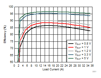
VPIN = VAVIN = 12 V, TA = 25 ºC, RRT = 40.2 kΩ (unless otherwise specified). Safe operating area curves were measured using a Texas Instruments evaluation module (EVM).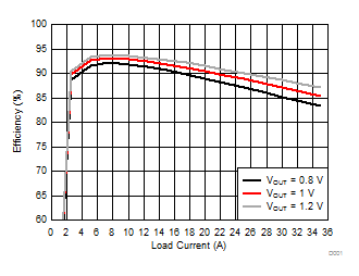
| VIN = 5 V | L = 300 nH | Snubber = 1 nF + 1Ω |
| fSW = 300 kHz | RDCR = 0.2 mΩ | RBOOT = 0 Ω |
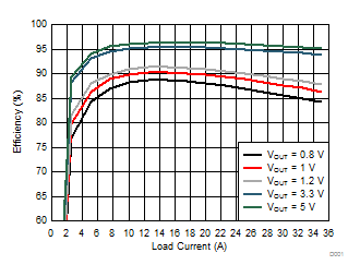
| VIN = 12 V | L = 300 nH | Snubber = 1 nF + 1Ω |
| fSW = 300 kHz | RDCR = 0.2 mΩ | RBOOT = 0 Ω |
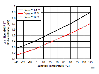 Figure 5. Low-Side MOSFET On-Resistance (RDS(on))
 vs Junction Temperature
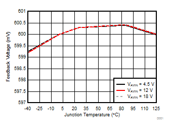
| VFB = 600 mV |
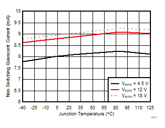
vs Junction Temperature
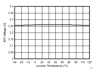
| IBP3 = 5 mA | VPVIN = VAVIN= 12 V |
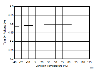
| VIN_ON = 4.5 V |
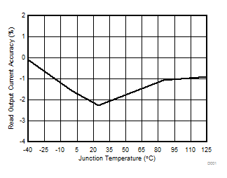
| IOUT = 20 A | VPVIN = VAVIN= 12 V |
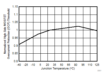
| BOOT – SW = 6.5 V | VPVIN = VAVIN= 12 V |
vs Junction Temperature
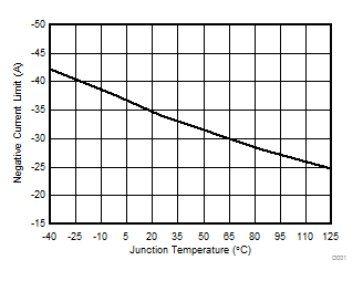
vs Junction Temperature
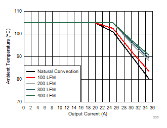
| VIN = 12 V | VOUT = 1 V | fSW = 300 kHz |
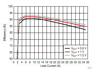
| VIN = 5 V | L = 300 nH | Snubber = 1 nF + 1Ω |
| fSW = 500 kHz | RDCR = 0.2 mΩ | RBOOT = 0 Ω |
| VIN = 12 V | L = 300 nH | Snubber = 1 nF + 1Ω |
| fSW = 500 kHz | RDCR = 0.2 mΩ | RBOOT = 0 Ω |
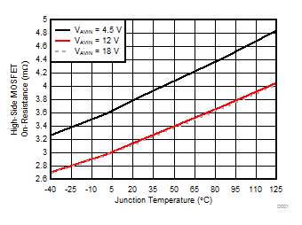 Figure 6. High-Side MOSFET On-Resistance (RDS(on))
 vs Junction Temperature
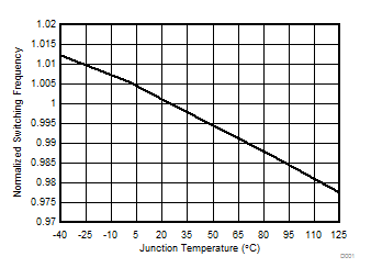
vs Junction Temperature
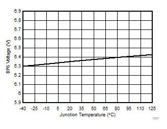
| IBP6 = 10 mA | VPVIN = VAVIN= 12 V |
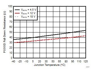
vs Junction Temperature
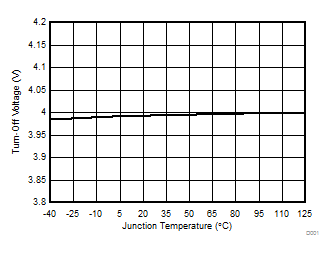
| VIN_OFF = 4 V |
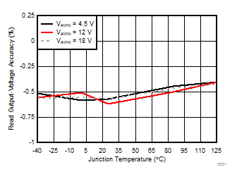
| VPVIN = VAVIN= 12 V |
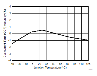
| OCF = 20 A | VPVIN = VAVIN= 12 V |
vs Junction Temperature
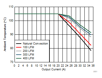
| VIN = 5 V | VOUT = 1 V | fSW = 300 kHz |
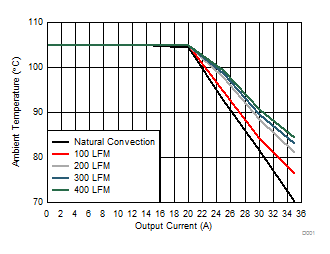
| VIN = 12 V | VOUT = 1 V | fSW = 500 kHz |