| INPUT SUPPLY |
| VAVIN |
Input supply voltage range |
|
4.5 |
|
18 |
V |
| VPVIN |
Power stage voltage range |
|
4.5 |
|
18 |
| IAVIN |
Input Operating Current |
Not switching |
|
7.7 |
12 |
mA |
| UVLO |
| VIN_ON |
Input turnon voltage |
Factory default setting |
|
4.5 |
|
V |
| Programmable range, 15 different settings |
4.25 |
|
7.75 |
| Accuracy |
–5% |
|
5% |
|
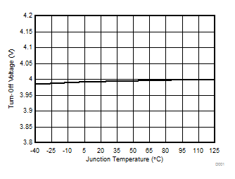
| VIN_OFF |
Input turnoff voltage |
Factory default setting |
|
4 |
|
V |
| Programmable range, 15 different settings |
4 |
|
7.5 |
| Accuracy |
–5% |
|
5% |
|
| ERROR AMPLIFIER AND FEEDBACK VOLTAGE |
| VFB |
Feedback pin voltage |
Default setting |
|
600 |
|
mV |
| Setpoint range(1) |
0.35 |
|
1.65 |
V |
| Setpoint resolution(1) |
|
2-9 |
|
V |
| VFB(ACC) |
Feedback pin voltage accuracy |
VFB = 600 mV, 0°C ≤ TJ ≤ 85°C(2) |
–0.5% |
|
0.5% |
% |
| VFB = 600 mV, -40°C ≤ TJ ≤ 125°C(2) |
–1% |
|
1% |
| VFB = 1650 mV, -40°C ≤ TJ ≤ 125°C(2) |
–1% |
|
1% |
| VFB = 350 mV, -40°C ≤ TJ ≤ 125°C(2) |
–1.5% |
|
1.5% |
| AOL |
Open-loop gain(1) |
|
80 |
|
|
dB |
| GBWP |
Gain bandwidth product(1) |
|
15 |
|
|
MHz |
| IFB |
FB pin input bias current |
VFB = 0.6 V |
-75 |
|
75 |
nA |
| ICOMP |
Sourcing |
VFB = 0 V |
1 |
|
|
mA |
| Sinking |
VFB = 1.2 V |
1 |
|
|
mA |
| OSCILLATOR |
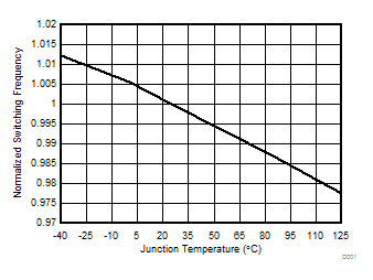
| fSW |
Adjustment range(2) |
|
200 |
|
1000 |
kHz |
|
Switching frequency(2) |
RRT = 40.2 kΩ |
450 |
500 |
550 |
kHz |
| VRMP |
Ramp peak-to-peak(1) |
|
|
VAVIN/6.5 |
|
V |
| VVLY |
Valley voltage(1) |
|
|
1.23 |
|
V |
| SYNCHRONIZATION |
| VIH(sync) |
High-level input voltage |
|
2.2 |
|
|
V |
| VIL(sync) |
Low-level input voltage |
|
|
|
0.80 |
V |
| Tpw(sync) |
Sync input iminimum pulse width |
Fsw = 160kHz to 1.2MHz |
|
|
200 |
ns |
| TMdelay(sync) |
Delay from the rising edge of SYNC input to the SW rising edge of the loop master device |
|
|
515 |
|
ns |
| TS delay(sync) |
Delay from the falling edge of SYNC input to the SW rising edge of the loop slave device |
|
|
515 |
|
ns |
| fSYNC |
Synchronization frequency |
|
160 |
|
1200 |
kHz |
| ΔfSYNC |
SYNC pin frequency range from free running frequency(1) |
|
–20% |
|
20% |
|
| RESET |
| VIH(reset) |
High-level input voltage(1) |
|
1.35 |
|
|
V |
| VIL(reset) |
Low-level input voltage |
|
|
|
0.8 |
| Tpw(reset) |
Minimum RESET_B pulse width |
|
200 |
|
|
ns |
| BP6 REGULATOR |
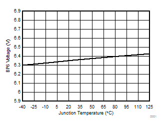
| VBP6 |
Regulator output voltage |
IBP6 = 10 mA |
5.85 |
6.4 |
6.95 |
V |
| VBP6(do) |
Regulator dropout voltage |
VAVIN – VBP6, VAVIN = 4.5 V, IBP6 = 25 mA |
100 |
200 |
400 |
mV |
| IBP6SC |
Regulator short-circuit current(1) |
VAVIN = 12 V |
|
150 |
|
mA |
| VBP6UV |
Regulator UVLO voltage(1) |
|
|
3.73 |
|
V |
| VBP6UV(hyst) |
Regulator UVLO voltage hysteresis(1) |
|
|
270 |
|
mV |
| BOOTSTRAP |
| VBOOT(drop) |
Bootstrap voltage drop |
IBOOT = 5 mA |
|
|
150 |
mV |
| BP3 REGULATOR |
| VBP3 |
3-V regulator output voltage |
VAVIN ≥ 4.5 V, IBP3 = 5 mA |
3 |
3.2 |
3.4 |
V |
| IBP3SC |
3-V regulator short-circuit current(1) |
|
18 |
35 |
|
mA |
| PWM |
| TON(min) |
Minimum controllable pulse width(1) |
|
|
|
100 |
ns |
| TOFF(min) |
Minimum off-time(1) |
|
|
515 |
550 |
ns |
| SOFT START |
| TON_RISE |
Soft-start time |
Factory default setting |
|
3 |
|
ms |
| Programmable range, 16 discrete settings(1) (3) |
0 |
|
100 |
| Accuracy, TON_RISE = 3 ms, VOUT_COMMAND = 0.95 V |
–10% |
|
10% |
|
| TON_MAX_FAULT_LIMIT |
Upper limit on the time to power up the output |
Factory default setting(4) |
|
0 |
|
ms |
| Programmable range, 16 discrete settings(1) (4) |
0 |
|
100 |
| Accuracy(1) |
–10% |
|
10% |
|
| TON_DELAY |
Turn-on delay |
Factory default setting |
|
0 |
|
ms |
| Programmable range, 16 discrete settings(1) |
0 |
|
100 |
| Accuracy(1) |
–10% |
|
10% |
|
| SOFT STOP |
| TOFF_FALL |
Soft-stop time |
Factory default setting(5) |
|
0 |
|
ms |
| Programmable range, 16 discrete settings(1) (5) |
0 |
|
100 |
| Accuracy, TOFF_FALL = 1 ms, VOUT_COMMAND = 0.95V |
–10% |
|
10% |
|
| TOFF_DELAY |
Turn-off delay |
Factory default setting |
|
0 |
|
ms |
| Programmable range, 16 discrete settings(1) |
0 |
|
100 |
| Accuracy(1) |
–10% |
|
10% |
|
| REMOTE SENSE AMPLIFIER |
| VDIFFO(ERROR) |
Error Voltage from DIFFO to (RSP – RSN) |
(VRSP – VRSN) = 0.6 V |
–4 |
|
4 |
mV |
| (VRSP – VRSN) = 1.2 V |
–5 |
|
5 |
| (VRSP – VRSN) = 3 V |
–15 |
|
15 |
| BW |
Closed-loop bandwidth(1) |
|
2 |
|
|
MHz |
| VDIFFO(max) |
Maximum DIFFO output voltage |
|
|
|
VBP6–0.2 |
V |
| IDIFFO |
DIFFO sourcing current |
|
1 |
|
|
mA |
| DIFFO sinking current |
|
1 |
|
|
mA |
| POWER STAGE |
| RHS |
High-side power device on-resistance |
VBOOT - VSW = 4.5 V, TJ = 25°C |
|
3.5 |
|
mΩ |
| VBOOT - VSW = 6.3V, TJ = 25°C |
|
3.2 |
|
mΩ |
| RLS |
Low-side power device on-resistance |
VAVIN = 4.5 V, TJ = 25°C |
|
1.5 |
|
mΩ |
| VAVIN ≥ 12 V, TJ = 25°C |
|
1.4 |
|
mΩ |
| TDEAD(LtoH) |
Power stage driver dead-time from Low-side off to High-side on |
VAVIN ≥ 12 V, TJ = 25°C(1) |
|
15 |
|
ns |
| TDEAD(HtoL) |
Power stage driver dead-time from High-side off to Low-side on |
VAVIN ≥ 12 V, TJ = 25°C(1) |
|
15 |
|
ns |
| CURRENT SHARING |
| ISHARE(acc) |
Output current sharing accuracy of two devices defined as the ratio of the current difference between two devices to the total current |
IOUT ≥ 20 A per device |
–15% |
|
15% |
|
| Output current sharing accuracy of two devices defined as the current difference between each device and the half of total current |
IOUT < 20 A per device |
–3 |
|
3 |
A |
| LOW-SIDE CURRENT LIMIT PROTECTION |
| tOFF(OC) |
Off time between restart attempts(1) |
|
|
7 × TON_RISE |
|
ms |
| IOUT_OC_FAULT_LIMIT |
Output current overcurrent fault threshold |
Factory default setting |
|
42 |
|
A |
| Programmable range |
5 |
|
52 |
| INEGOC |
Negative output current overcurrent protection threshold |
|
–60 |
-40 |
–20 |
A |
| IOUT_OC_WARN_LIMIT |
Output current overcurrent warning threshold |
Factory default setting |
|
37 |
|
A |
| Programmable range |
4 |
|
50 |
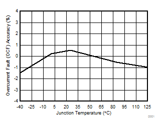
| IOC(acc) |
Output current overcurrent fault accuracy |
IOUT ≥ 20 A |
–15% |
|
15% |
|
| HIGH-SIDE SHORT CIRCUIT PROTECTION |
| IHSOC |
High-side short-circuit protection fault threshold |
(VBOOT-VSW) = 6.3V, TJ = 25°C |
|
65 |
|
A |
| POWER GOOD (PGOOD) AND OVERVOLTAGE/UNDERVOLTAGE WARNING |
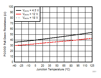
| RPGD |
PGD pulldown resistance |
VDIFFO = 0, IPGD = 5 mA |
|
45 |
60 |
Ω |
| IPGD(OH) |
Output high open drain leakage current into PGD pin |
VPGD = 5 V |
|
|
15 |
µA |
| VPGD(OL) |
PGD pin output low level voltage at no supply voltage |
VAVIN=0, IPGD = 80 μA |
|
|
0.8 |
V |
| VFBOVW |
Overvoltage warning threshold at FB pin (PGD fault threshold on rising) |
Factory default, at VREF = 600 mV |
108 |
112 |
116 |
% VREF |
| VFBUVW |
Undervoltage warning threshold at FB pin (PGD fault threshold on falling) |
Factory default, at VREF = 600 mV |
84 |
88 |
92 |
% VREF |
| VPGD(rise) |
PGD good threshold on rising and Undervotlage warning threshold de-assertation threshold at FB pin |
VREF = 600 mV |
|
95 |
|
% VREF |
| VPGD(fall) |
PGD good threshold on falling and Overvotlage warning threshold de-assertation threshold at FB pin |
VREF = 600 mV |
|
105 |
|
% VREF |
| OUTPUT OVERVOLTAGE AND UNDERVOLTAGE FAULT PROTECTION |
| VFBOVF |
Overvoltage fault threshold at FB pin |
Factory default, at VREF = 600 mV |
113 |
117 |
121 |
% VREF |
| VFBUVF |
Undervoltage fault threshold at FB pin |
Factory default, at VREF = 600mV |
79 |
83 |
87 |
% VREF |
| OUTPUT VOLTAGE TRIMMIN8 |
| VFBRES |
Resolution of FB steps with VOUT_COMMAND, Trim and Margin |
|
|
2-9 |
|
V |
| VOUT_TRANSITION_RATE |
Output voltage transition rate |
Factory default setting |
|
1 |
|
mV/µs |
| Programmable range, 8 discrete settings |
0.067 |
|
1.5 |
| Accuracy |
–10% |
|
10% |
|
| VOUT_SCALE_LOOP |
Feedback loop scaling factor |
Factory default setting |
|
1 |
|
|
| Programmable range, 3 discrete settings |
0.25 |
|
1 |
| VOUT_COMMAND |
Output voltage programmable register value, multiply by 2-9 to get output voltage |
Factor default setting |
|
307 |
|
|
| Programmable range |
VOUT_SCALE_LOOP = 1 |
179 |
|
845 |
| VOUT_SCALE_LOOP = 0.5(1) |
358 |
|
1690 |
| VOUT_SCALE_LOOP = 0.25(1) |
716 |
|
2816 |
| TEMPERATURE SENSE AND THERMAL SHUTDOWN |
| TSD |
Junction thermal shutdown temperature(1) |
|
135 |
145 |
160 |
°C |
| THYST |
Junction thermal shutdown hysteresis(1) |
|
|
25 |
|
°C |
| OT_FAULT_LIMIT |
Internal overtemperature fault limit(1) |
Factory default setting |
|
145 |
|
°C |
| Programmable range |
120 |
|
165 |
| OT_WARN_LIMIT |
Internal overtemperature warning limit(1) |
Factory default setting |
|
120 |
|
°C |
| Programmable range |
100 |
|
140 |
| TOT(hys) |
Internal overtemperature fault, warning hysteresis(1) |
|
15 |
20 |
25 |
°C |
| MEASUREMENT SYSTEM |
| MVOUT(rng) |
Output voltage measurement range(1) |
|
0 |
|
5.8 |
V |
| MVOUT(acc) |
Output voltage measurement accuracy |
DIFFO = 1.2 V |
–2% |
|
2% |
% |
| MVOUT(lsb) |
Output voltage measurement bit resolution(1) |
|
|
2-9 |
|
V |
| MIOUT(rng) |
Output current measurement range(1) |
|
0 |
|
52 |
A |
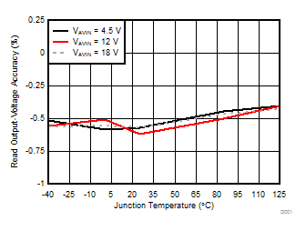
| MIOUT(acc) |
Output current measurement accuracy |
IOUT 20 A, TJ= 25°C |
–10% |
0 |
10% |
|
| IOUT ≥ 20 A |
–15% |
|
15% |
| 3A ≤ IOUT <20 A |
–3 |
|
3 |
A |
| MIOUT(lsb) |
Output current measurement bit resolution(1) |
|
|
62.5 |
|
mA |
| MTSNS(rng) |
Internal temperature sense range(1) |
|
-40 |
|
165 |
°C |
| MTSNS(acc) |
Internal temperature sense accuracy(1) |
-40°C ≤ TJ ≤ 165°C |
–5 |
|
5 |
°C |
| MTSNS(lsb) |
Internal temperature sense bit resolution(1) |
|
|
1 |
|
°C |
| PMBUS INTERFACE |
| VIH(PMBUS) |
High-level input voltage on PMB_CLK, PMB_DATA, CNTL |
|
1.35 |
|
|
V |
| VIL(PMBUS) |
Low-level input voltage on PMB_CLK, PMB_DATA, CNTL |
|
|
|
0.8 |
V |
| VhysCNTL |
Hysteresis on CNTL |
|
|
170 |
|
mV |
| IIH(PMBUS) |
Input high level current into PMB_CLK, PMB_DATA |
|
–10 |
|
10 |
μA |
| IIL(PMBUS) |
Input low level current into PMB_CLK, PMB_DATA |
|
–10 |
|
10 |
μA |
| ICNTL |
CNTL pin pullup current |
|
5 |
|
10 |
μA |
| VOL(PMBUS) |
Output low level voltage on PMB_DATA, SMB_ALRT |
VAVIN > 4.5 V, input current to PMB_DATA, SMB_ALRT = 4 mA |
|
|
0.4 |
V |
| IOH(PMBUS) |
Output high level open drain leakage current into PMB_DATA, SMB_ALRT |
Voltage on PMB_DATA, SMB_ALRT = 5.5 V |
|
|
10 |
μA |
| IOL(PMBUS) |
Output low level open drain leakage current into PMB_DATA, SMB_ALRT |
Voltage on PMB_DATA, SMB_ALRT < 0.4 V |
4 |
|
|
mA |
| FPMBUS |
PMBus operating frequency range |
Slave mode |
10 |
|
400 |
kHz |
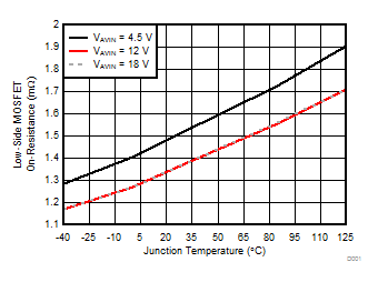 Figure 5. Low-Side MOSFET On-Resistance (RDS(on))
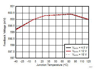
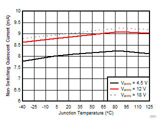
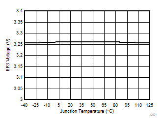
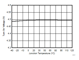
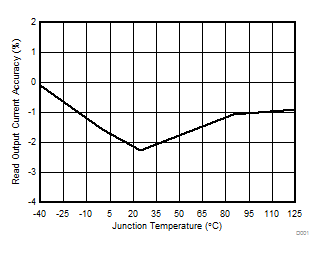
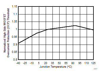
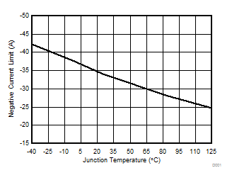
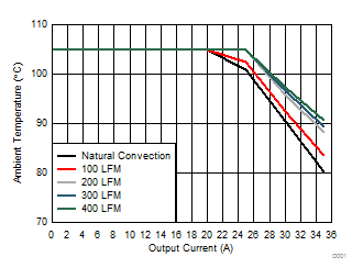
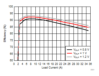
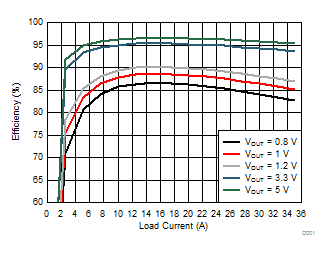
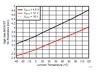 Figure 6. High-Side MOSFET On-Resistance (RDS(on))