ZHCSG55A November 2016 – February 2017 TPS54824
PRODUCTION DATA.
- 1 特性
- 2 应用
- 3 说明
- 4 修订历史记录
- 5 Pin Configuration and Functions
- 6 Specifications
-
7 Detailed Description
- 7.1 Overview
- 7.2 Functional Block Diagram
- 7.3
Feature Description
- 7.3.1 Fixed Frequency PWM Control
- 7.3.2 Continuous Conduction Mode Operation (CCM)
- 7.3.3 VIN Pins and VIN UVLO
- 7.3.4 Voltage Reference and Adjusting the Output Voltage
- 7.3.5 Error Amplifier
- 7.3.6 Enable and Adjustable UVLO
- 7.3.7 Soft Start and Tracking
- 7.3.8 Safe Start-up into Pre-Biased Outputs
- 7.3.9 Power Good
- 7.3.10 Sequencing (SS/TRK)
- 7.3.11 Adjustable Switching Frequency (RT Mode)
- 7.3.12 Synchronization (CLK Mode)
- 7.3.13 Bootstrap Voltage and 100% Duty Cycle Operation (BOOT)
- 7.3.14 Output Overvoltage Protection (OVP)
- 7.3.15 Overcurrent Protection
- 7.4 Device Functional Modes
-
8 Application and Implementation
- 8.1 Application Information
- 8.2
Typical Application
- 8.2.1 Design Requirements
- 8.2.2
Detailed Design Procedure
- 8.2.2.1 Switching Frequency
- 8.2.2.2 Output Inductor Selection
- 8.2.2.3 Output Capacitor
- 8.2.2.4 Input Capacitor
- 8.2.2.5 Output Voltage Resistors Selection
- 8.2.2.6 Soft-start Capacitor Selection
- 8.2.2.7 Undervoltage Lockout Set Point
- 8.2.2.8 Bootstrap Capacitor Selection
- 8.2.2.9 PGOOD Pull-up Resistor
- 8.2.2.10 Compensation
- 8.2.3 Application Curves
- 9 Power Supply Recommendations
- 10Layout
- 11器件和文档支持
- 12机械、封装和可订购信息
10 Layout
10.1 Layout Guidelines
- VIN and PGND traces should be as wide as possible to reduce trace impedance and improve heat dissipation.
- An input capacitor is required on both VIN pins of the IC and must be placed as close as possible to the IC.
- The PGND trace between the output capacitor and the PGND pin should be as wide as possible to minimize its trace impedance.
- Provide sufficient vias for the input capacitor and output capacitor.
- Keep the SW trace as physically short and wide as practical to minimize radiated emissions.
- A separate VOUT path should be connected to the upper feedback resistor.
- Voltage feedback loop should be placed away from the high-voltage switching trace. It is preferable to use ground copper near it as a shield.
- The trace connected to the FB node should be as small as possible to avoid noise coupling.
- Place components connected to the RT/CLK, FB, COMP and SS/TRK pins as close to the IC as possible and minimize traces connected to these pins to avoid noise coupling.
- AGND must be connected to PGND on the PCB. Connect AGND to PGND in a region away from switching currents.
10.2 Layout Example
Figure 51 through Figure 54 shows an example PCB layout and the following list provides a description of each layer.
- The top layer has all components and the main traces for VIN, SW, VOUT and PGND. Both VIN pins are bypassed with two input capacitors placed as close as possible to the IC. Multiple vias are placed near the input and output capacitors. The AGND trace is connected to PGND with a wide trace away from the input capacitors to minimize switching noise.
- Midlayer 1 is used to route the BOOT pin to the BOOT-SW capacitor (CBT). The rest of this layer is covered with PGND.
- Midlayer 2 has a wide trace connecting both VIN pins of the IC. It also has a parallel trace for VOUT to minimize trace resistance. The rest of this layer is covered with PGND.
- The bottom layer has the trace connecting the FB resistor divider to VOUT at the point of regulation. PGND is filled into the rest of this layer to aid with thermal performance.
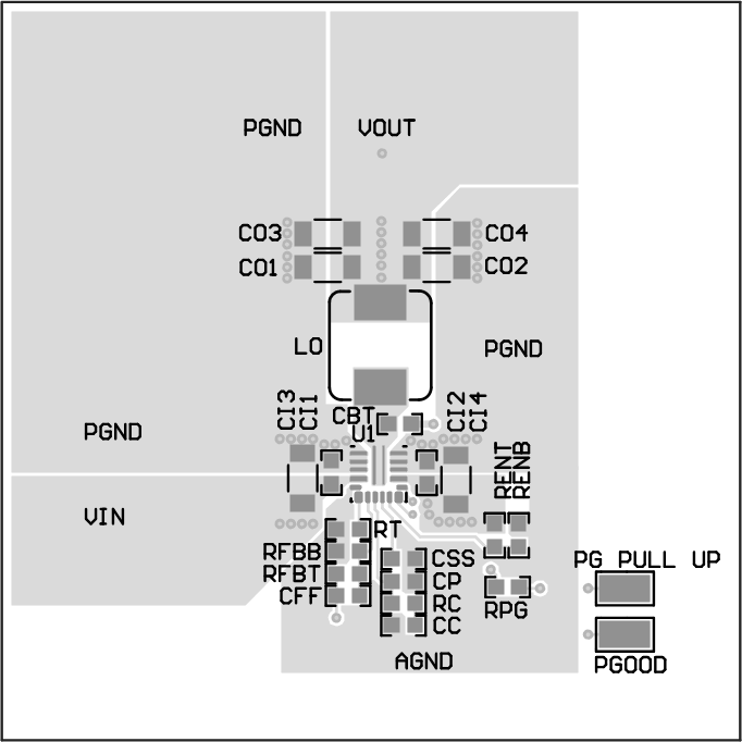 Figure 51. TPS54824 Layout Top
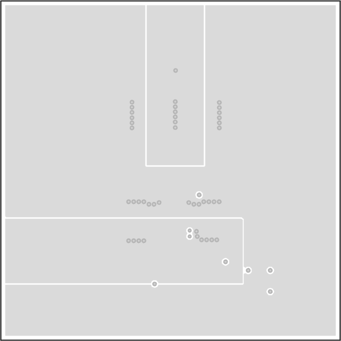 Figure 53. TPS54824 Layout Midlayer 2
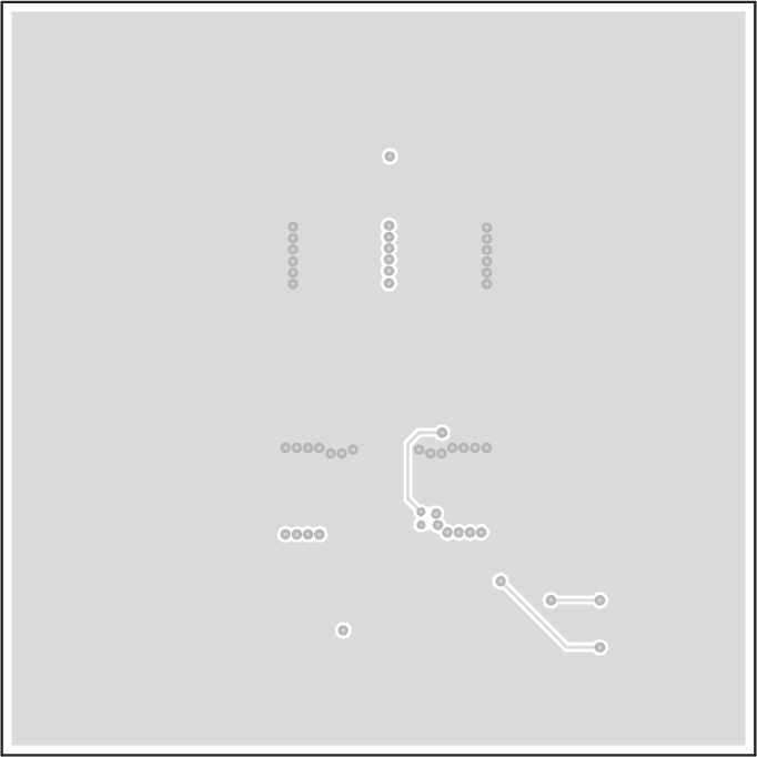 Figure 52. TPS54824 Layout Midlayer 1
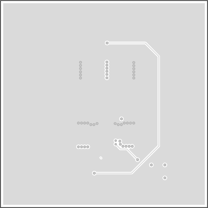 Figure 54. TPS54824 Layout Bottom
10.3 Alternate Layout Example
Figure 55 through Figure 58 shows an alternate example PCB layout with unsymmetrical placement of the input capacitors and output capacitors. Both VIN pins are still bypassed with an input capacitor placed as close as possible to the IC.
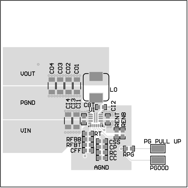 Figure 55. TPS54824 Alternate Layout Top
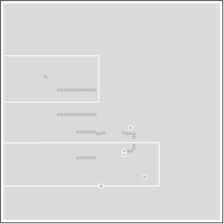 Figure 57. TPS54824 Alternate Layout Midlayer 2
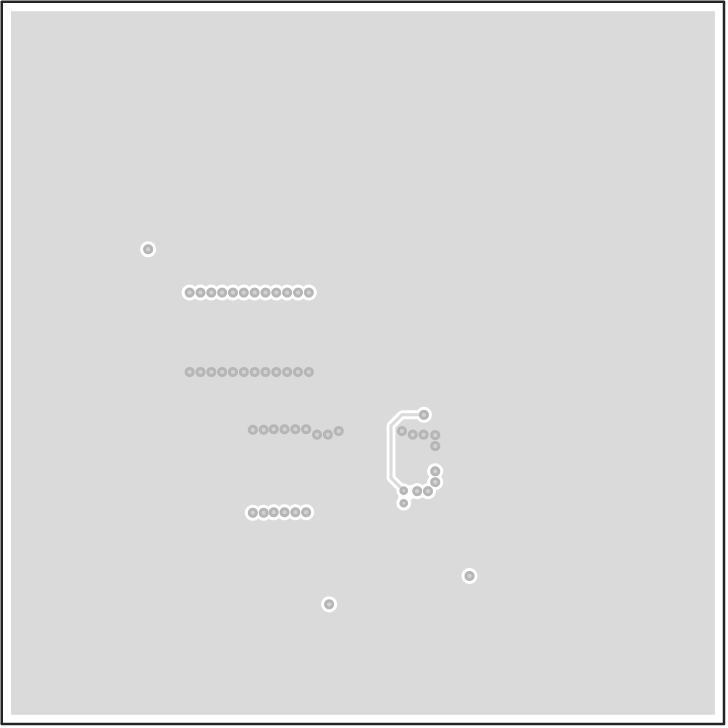 Figure 56. TPS54824 Alternate Layout Midlayer 1
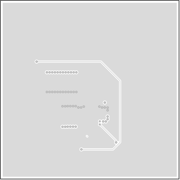 Figure 58. TPS54824 Alternate Layout Bottom