ZHCSG55A November 2016 – February 2017 TPS54824
PRODUCTION DATA.
- 1 特性
- 2 应用
- 3 说明
- 4 修订历史记录
- 5 Pin Configuration and Functions
- 6 Specifications
-
7 Detailed Description
- 7.1 Overview
- 7.2 Functional Block Diagram
- 7.3
Feature Description
- 7.3.1 Fixed Frequency PWM Control
- 7.3.2 Continuous Conduction Mode Operation (CCM)
- 7.3.3 VIN Pins and VIN UVLO
- 7.3.4 Voltage Reference and Adjusting the Output Voltage
- 7.3.5 Error Amplifier
- 7.3.6 Enable and Adjustable UVLO
- 7.3.7 Soft Start and Tracking
- 7.3.8 Safe Start-up into Pre-Biased Outputs
- 7.3.9 Power Good
- 7.3.10 Sequencing (SS/TRK)
- 7.3.11 Adjustable Switching Frequency (RT Mode)
- 7.3.12 Synchronization (CLK Mode)
- 7.3.13 Bootstrap Voltage and 100% Duty Cycle Operation (BOOT)
- 7.3.14 Output Overvoltage Protection (OVP)
- 7.3.15 Overcurrent Protection
- 7.4 Device Functional Modes
-
8 Application and Implementation
- 8.1 Application Information
- 8.2
Typical Application
- 8.2.1 Design Requirements
- 8.2.2
Detailed Design Procedure
- 8.2.2.1 Switching Frequency
- 8.2.2.2 Output Inductor Selection
- 8.2.2.3 Output Capacitor
- 8.2.2.4 Input Capacitor
- 8.2.2.5 Output Voltage Resistors Selection
- 8.2.2.6 Soft-start Capacitor Selection
- 8.2.2.7 Undervoltage Lockout Set Point
- 8.2.2.8 Bootstrap Capacitor Selection
- 8.2.2.9 PGOOD Pull-up Resistor
- 8.2.2.10 Compensation
- 8.2.3 Application Curves
- 9 Power Supply Recommendations
- 10Layout
- 11器件和文档支持
- 12机械、封装和可订购信息
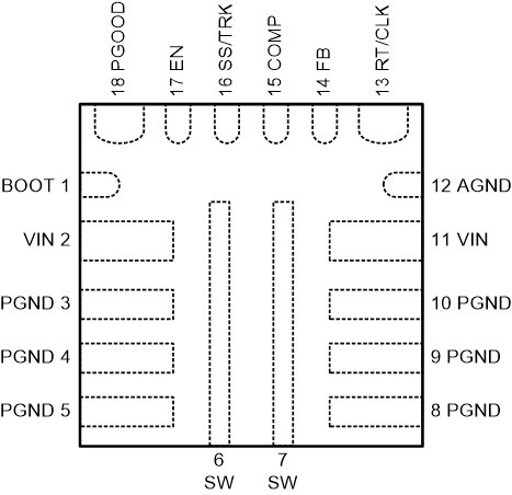
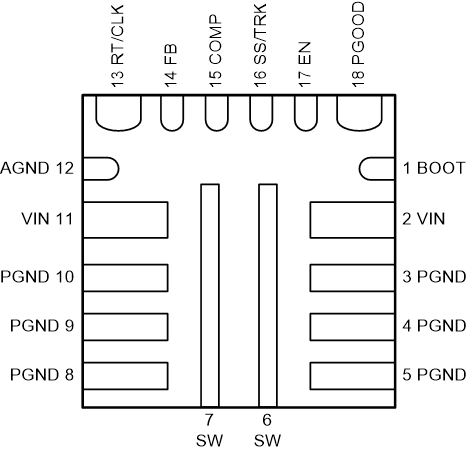
5 Pin Configuration and Functions
RNV Package
18-Pin VQFN-HR
Top View

Bottom View

Pin Functions
| PIN | I/O | DESCRIPTION | |
|---|---|---|---|
| NAME | NO. | ||
| BOOT | 1 | I | Floating supply voltage for high-side MOSFET gate drive circuit. Connect a 0.1-µF ceramic capacitor between BOOT and SW pins. |
| VIN | 2, 11 | I | Input voltage supply pin. Power for the internal circuit and the connection to drain of high-side MOSFET. Connect both pins to the input power source with a low impedance connection. Connect both pins and their neighboring PGND pins. |
| PGND | 3, 4, 5, 8, 9, 10 | – | Ground return for low-side power MOSFET and its drivers. |
| SW | 6, 7 | O | Switching node. Connected to the source of the high-side MOSFET and drain of the low-side MOSFET. |
| AGND | 12 | – | Ground of internal analog circuitry. AGND must be connected to the PGND plane. |
| RT/CLK | 13 | I | Switching frequency setting pin. In RT mode, an external timing resistor adjusts the switching frequency. In CLK mode, the device synchronizes to an external clock input to this pin. |
| FB | 14 | I | Converter feedback input. Connect to the output voltage with a resistor divider. |
| COMP | 15 | I | Error amplifier output and input to the PWM modulator. Connect loop compensation to this pin. |
| SS/TRK | 16 | I | Soft-start and tracking pin. Connecting an external capacitor sets the soft-start time. This pin can also be used for tracking and sequencing. |
| EN | 17 | I | Enable pin. Float or pull high to enable the device. Connect a resistor divider to this pin to implement adjustable under voltage lockout and hysteresis. |
| PGOOD | 18 | O | Open-drain power good indicator. It is asserted low if output voltage is outside if the PGOOD thresholds, VIN is low, EN is low, device is in thermal shutdown or device is in soft-start. |