ZHCSEL7A November 2015 – December 2015 TPS548A20
PRODUCTION DATA.
- 1 特性
- 2 应用
- 3 说明
- 4 修订历史记录
- 5 Pin Configuration and Functions
- 6 Specifications
-
7 Detailed Description
- 7.1 Overview
- 7.2 Functional Block Diagrams
- 7.3
Feature Description
- 7.3.1 Powergood
- 7.3.2 D-CAP3 Control and Mode Selection
- 7.3.3 D-CAP3 Mode
- 7.3.4 Sample and Hold Circuitry
- 7.3.5 Adaptive Zero-Crossing
- 7.3.6 Forced Continuous-Conduction Mode
- 7.3.7 Current Sense and Overcurrent Protection
- 7.3.8 Overvoltage and Undervoltage Protection
- 7.3.9 Out-of-Bounds Operation (OOB)
- 7.3.10 UVLO Protection
- 7.3.11 Thermal Shutdown
- 7.4 Device Functional Modes
- 8 Application and Implementation
- 9 Power Supply Recommendations
- 10Layout
- 11器件和文档支持
- 12机械、封装和可订购信息
10 Layout
10.1 Layout Guidelines
Before beginning a design using the TPS548A20 , consider the following:
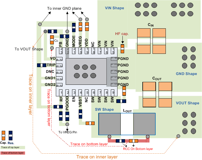
- Place the power components (including input and output capacitors, the inductor, and the TPS548A20 ) on the solder side of the PCB. In order to shield and isolate the small signal traces from noisy power lines, insert and connect at least one inner plane to ground.
- All sensitive analog traces and components such as VFB, PGOOD, TRIP, MODE, and ADDR must be placed away from high-voltage switching nodes such as SW and VBST to avoid coupling. Use internal layers as ground planes and shield the feedback trace from power traces and components.
- Pin 22 (GND pin) must be connected directly to the thermal pad. Connect the thermal pad to the PGND pins and then to the GND plane.
- Place the VIN decoupling capacitors as close to the VIN and PGND pins as possible to minimize the input AC-current loop.
- Place the feedback resistor near the IC to minimize the VFB trace distance.
- Place the frequency-setting resistor (ADDR), OCP-setting resistor (RTRIP) and mode-setting resistor (RMODE) close to the device. Use the common GND via to connect the resistors to the GND plane if applicable.
- Place the VDD and VREG decoupling capacitors as close to the device as possible. Provide GND vias for each decoupling capacitor and ensure the loop is as small as possible.
- The PCB trace is defined as switch node, which connects the SW pins and high-voltage side of the inductor. The switch node should be as short and wide as possible.
- Use separated vias or trace to connect SW node to the snubber, bootstrap capacitor, and ripple-injection resistor. Do not combine these connections.
- Place one more small capacitor (2.2 nF, 0402 size) between the VIN and PGND pins. This capacitor must be placed as close to the IC as possible.
- TI recommends placing a snubber between the SW shape and GND shape for effective ringing reduction. The value of snubber design starts at 3 Ω + 470 pF.
- Consider R-C-CC network (Ripple injection network) component placement and place the AC coupling capacitor, CC, close to the device, and R and C close to the power stage.
- See Figure 50 for the layout recommendation.
10.2 Layout Example
 Figure 50. Layout Recommendation