ZHCSOA1A July 2021 – July 2021 TPS548B27
PRODUCTION DATA
- 1 特性
- 2 应用
- 3 说明
- 4 Revision History
- 5 Pin Configuration and Functions
- 6 Specifications
-
7 Detailed Description
- 7.1 Overview
- 7.2 Functional Block Diagram
- 7.3
Feature Description
- 7.3.1 Internal VCC LDO and Using External Bias on VCC Pin
- 7.3.2 Enable
- 7.3.3 Output Voltage Setting
- 7.3.4 Internal Fixed Soft Start and External Adjustable Soft Start
- 7.3.5 External REFIN For Output Voltage Tracking
- 7.3.6 Frequency and Operation Mode Selection
- 7.3.7 D-CAP3 Control
- 7.3.8 Low-Side FET Zero-Crossing
- 7.3.9 Current Sense and Positive Overcurrent Protection
- 7.3.10 Low-Side FET Negative Current Limit
- 7.3.11 Power Good
- 7.3.12 Overvoltage and Undervoltage Protection
- 7.3.13 Out-Of-Bounds (OOB) Operation
- 7.3.14 Output Voltage Discharge
- 7.3.15 UVLO Protection
- 7.3.16 Thermal Shutdown
- 7.4 Device Functional Modes
-
8 Application and Implementation
- 8.1 Application Information
- 8.2
Typical Application
- 8.2.1 Design Requirements
- 8.2.2
Detailed Design Procedure
- 8.2.2.1 Output Voltage Setting Point
- 8.2.2.2 Choose the Switching Frequency and the Operation Mode
- 8.2.2.3 Choose the Inductor
- 8.2.2.4 Set the Current Limit (TRIP)
- 8.2.2.5 Choose the Output Capacitor
- 8.2.2.6 Choose the Input Capacitors (CIN)
- 8.2.2.7 Soft-Start Capacitor (SS/REFIN Pin)
- 8.2.2.8 EN Pin Resistor Divider
- 8.2.2.9 VCC Bypass Capacitor
- 8.2.2.10 BOOT Capacitor
- 8.2.2.11 PGOOD Pullup Resistor
- 8.2.3 Application Curves
- 9 Power Supply Recommendations
- 10布局
- 11Device and Documentation Support
- 12Mechanical, Packaging, and Orderable Information
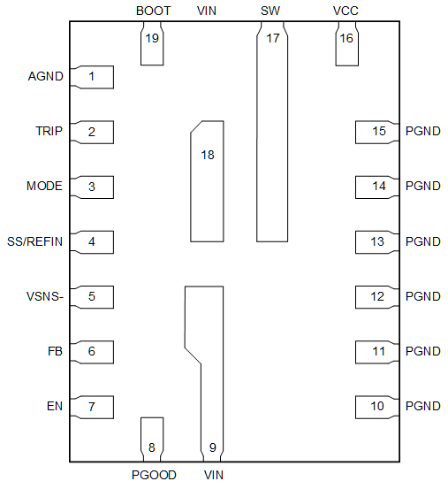
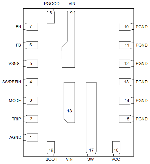
5 Pin Configuration and Functions
 Figure 5-1 RYL Package, 19-Pin VQFN-FCRLF
(Top View)
 Figure 5-2 RYL Package, 19-Pin VQFN-FCRLF
 (Bottom View)
Table 5-1 Pin Functions
| NAME | NO. | I/O(1) | DESCRIPTION |
|---|---|---|---|
| BOOT | 19 | I/O | Supply rail for the high-side gate driver (boost terminal). Connect the bootstrap capacitor from this pin to SW node. |
| AGND | 1 | G | Ground pin. Reference point for the internal control circuits |
| TRIP | 2 | I/O | Current limit setting pin. Connect a resistor to AGND to set the current limit trip point. ±1% tolerance resistor is highly recommended. See Section 7.3.9 for details on the OCL setting. |
| MODE | 3 | I | The MODE pin sets the Forced Continuous Conduction mode (FCCM) or Skip mode operation. It also selects the operating frequency by connecting a resistor from the MODE pin to AGND. ±1% tolerance resistor is recommended. See Table 7-1 for details. |
| SS/REFIN | 4 | I/O | Dual-function pin Soft-start function: Connecting a capacitor to the VSNS– pin programs the soft-start time. Minimum soft-start time (1.5 ms) is fixed internally. A minimum 1-nF capacitor is required for this pin to avoid overshoot during the charge of the soft-start capacitor. REFIN function: The device always looks at the voltage on this SS/REFIN pin as the reference for the control loop. The internal reference voltage can be overridden by an external DC voltage source on this pin for tracking application. |
| VSNS– | 5 | I | The return connection for a remote voltage sensing configuration. It is also used as ground for the internal reference. Short to AGND for a single-end sense configuration. |
| FB | 6 | I | Output voltage feedback input. A resistor divider from VOUT to VSNS– (tapped to FB pin) sets the output voltage. |
| EN | 7 | I | Enable pin (EN). The Enable pin turns the DC/DC switching converter on or off. Floating the EN pin before start-up disables the converter. The maximum recommended operating condition for the EN pin is 5.5 V. Do not connect the EN pin to the VIN pin directly. |
| PGOOD | 8 | O | Open-drain power-good status signal. When FB voltage moves outside the specified limits, PGOOD goes low after a 2-µs delay. |
| VIN | 9,18 | P | Power-supply input pins for both integrated power MOSFET pair and the internal LDO. Place the decoupling input capacitors from the VIN pins to the PGND pins as close as possible. |
| PGND | 10,11,12,13,14,15 | G | Power ground of the internal low-side MOSFET. At least six PGND vias are required to be placed as close as possible to the PGND pins. This minimizes parasitic impedance and lowers thermal resistance. |
| VCC | 16 | I/O | Internal 3-V LDO output. An external bias with 3.3-V or higher voltage can be connected to this pin to save the power losses on the internal LDO. The voltage source on this pin powers both the internal circuitry and gate driver. Requires a 2.2-µF, at least 6.3-V, rating ceramic capacitor from the VCC pin to the PGND pins as the decoupling capacitor and the placement is required to be as close as possible. |
| SW | 17 | O | Output switching terminal of the power converter. Connect this pin to the output inductor. |
(1) I = Input, O = Output, P = Supply, G = Ground