ZHCSMV4A December 2020 – December 2022 TPS548B28
PRODUCTION DATA
- 1 特性
- 2 应用
- 3 说明
- 4 Revision History
- 5 Pin Configuration and Functions
- 6 Specifications
-
7 Detailed Description
- 7.1 Overview
- 7.2 Functional Block Diagram
- 7.3
Feature Description
- 7.3.1 Internal VCC LDO And Using External Bias On VCC Pin
- 7.3.2 Enable
- 7.3.3 Output Voltage Setting
- 7.3.4 Internal Fixed Soft Start and External Adjustable Soft Start
- 7.3.5 External REFIN For Output Voltage Tracking
- 7.3.6 Frequency and Operation Mode Selection
- 7.3.7 D-CAP3™ Control Mode
- 7.3.8 Low-side FET Zero-Crossing
- 7.3.9 Current Sense and Positive Overcurrent Protection
- 7.3.10 Low-side FET Negative Current Limit
- 7.3.11 Power Good
- 7.3.12 Overvoltage and Undervoltage Protection
- 7.3.13 Out-Of-Bounds (OOB) Operation
- 7.3.14 Output Voltage Discharge
- 7.3.15 UVLO Protection
- 7.3.16 Thermal Shutdown
- 7.4 Device Functional Modes
-
8 Application and Implementation
- 8.1 Application Information
- 8.2
Typical Application
- 8.2.1 Design Requirements
- 8.2.2
Detailed Design Procedure
- 8.2.2.1 Output Voltage Setting Point
- 8.2.2.2 Choose the Switching Frequency and the Operation Mode
- 8.2.2.3 Choose the Inductor
- 8.2.2.4 Set the Current Limit (TRIP)
- 8.2.2.5 Choose the Output Capacitor
- 8.2.2.6 Choose the Input Capacitors (CIN)
- 8.2.2.7 Soft Start Capacitor (SS/REFIN Pin)
- 8.2.2.8 EN Pin Resistor Divider
- 8.2.2.9 VCC Bypass Capacitor
- 8.2.2.10 BOOT Capacitor
- 8.2.2.11 PGOOD Pullup Resistor
- 8.2.3 Application Curves
- 8.3 Power Supply Recommendations
- 8.4 Layout
- 9 Device and Documentation Support
- 10Mechanical, Packaging, and Orderable Information
7.4.5 Powering the Device From a Split-rail Configuration
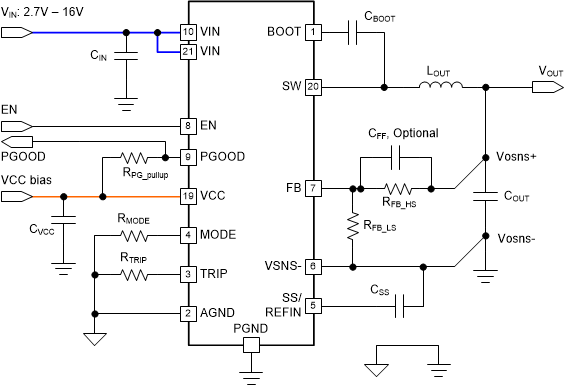
When an external bias, which is at a different level from main VIN bus, is applied onto the VCC pin, the device can be configured to split-rail by utilizing both the main VIN bus and VCC bias. Connecting a valid VCC bias to VCC pin overrides the internal LDO, thus saves power loss on that linear regulator. This configuration helps to improve overall system level efficiency but requires a valid VCC bias. A 3.3-V rail is the common choice as VCC bias. With a stable VCC bias, the VIN input range under this configuration can be as low as 2.7 V and up to 16 V.
The noise of the external bias affects the internal analog circuitry. To ensure a proper operation, a clean, low-noise external bias and good local decoupling capacitor from VCC pin to PGND pin are required. Figure 7-7 shows an example for this split rail configuration.
The VCC external bias current during nominal operation varies with the bias voltage level and also the operating frequency. For example, by setting the device to skip-mode, the VCC pins draw less and less current from the external bias when the frequency decreases under light load condition. The typical VCC external bias current under FCCM operation is listed in Section 6.5 to help you prepare the capacity of the external bias.
Under split rail configuration, VIN, VCC bias, and EN are the signals to enable the part. For start-up sequence, TI recommends that at least one of VIN UVLO rising threshold and EN rising threshold is satisfied later than VCC UVLO rising threshold. A practical start-up sequence example is: VIN applied first, the external bias applied, and then EN signal goes high.
 Figure 7-7 Split Rail Configuration With External VCC Bias