ZHCSEW7A December 2015 – April 2016 TPS54A20
PRODUCTION DATA.
- 1 特性
- 2 应用
- 3 说明
- 4 修订历史记录
- 5 Pin Configuration and Functions
- 6 Specifications
-
7 Detailed Description
- 7.1 Overview
- 7.2 Functional Block Diagram
- 7.3
Feature Description
- 7.3.1 Frequency Selection
- 7.3.2 External Clock Syncronization
- 7.3.3 Adjusting the Output Voltage
- 7.3.4 Soft Start
- 7.3.5 Startup into Pre-biased Outputs
- 7.3.6 Power Good (PGOOD)
- 7.3.7 Overcurrent Protection
- 7.3.8 Light Load Operation
- 7.3.9 Output Undervoltage/Overvoltage Protection
- 7.3.10 Input Undervoltage/Overvoltage Lockout
- 7.3.11 Enable and Adjusting Undervoltage Lockout
- 7.3.12 Series Capacitor Monitoring
- 7.3.13 Thermal Shutdown
- 7.3.14 Phase A Power Stage
- 7.3.15 Phase B Power Stage
- 7.3.16 Internal Gate Drive Regulator
- 7.3.17 Voltage Feed Forward
- 7.3.18 Internal Oscillator
- 7.3.19 Pulse Frequency Detector
- 7.3.20 On-Time Generator
-
8 Application and Implementation
- 8.1 Application Information
- 8.2
Typical Application
- 8.2.1 Design Requirements
- 8.2.2
Detailed Design Procedure
- 8.2.2.1 Output Voltage
- 8.2.2.2 Switching Frequency
- 8.2.2.3 On-Time
- 8.2.2.4 Inductor Selection
- 8.2.2.5 Output Capacitor Selection
- 8.2.2.6 Input Capacitor Selection
- 8.2.2.7 Series Capacitor Selection
- 8.2.2.8 Soft-Start Time Selection
- 8.2.2.9 Bootstrap Capacitor Selection
- 8.2.2.10 Gate Drive Capacitor Selection
- 8.2.2.11 Under Voltage Lockout Set Point
- 8.2.2.12 Current Limit Selection
- 8.2.3 Application Curves
- 9 Power Supply Recommendations
- 10Layout
- 11器件和文档支持
- 12机械、封装和可订购信息
10 Layout
10.1 Layout Guidelines
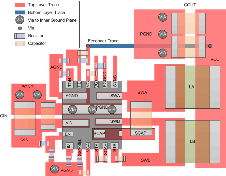
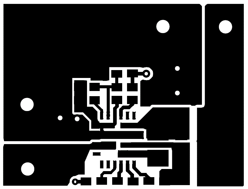
- Layout is a critical portion of good power supply design. See Figure 62 and Figure 63 for a PCB layout example. It may be possible to obtain acceptable performance with alternate PCB layouts, however this layout has been shown to produce good results and is meant as a guideline.
- The IC package design provides several quiet pads for heat removal and enables a tight layout of the board components.
- Place the power components (including input and output capacitors, inductors, the series capacitor, and the TPS54A20 device) on the solder side of the PCB. To shield and isolate the small signal traces from noisy power lines, insert and connect at least one inner plane to ground.
- All sensitive analog traces and components such as FB, EN, TON, PGOOD, ILIM, and SS/FSEL must be placed away from high-voltage switching nodes such as SWA, SWB, SCAP, BOOTA, and BOOTB to avoid coupling. Use internal layers as ground planes and shield the feedback trace from power traces and components.
- Care should be taken to minimize the loop area formed by the input bypass capacitor connections, the VIN pin, and the ground connections. Place the input capacitors right next to the IC. Use low ESR ceramic capacitors with X5R or X7R dielectric.
- Care should also be taken to minimize the loop area formed by the series capacitor. Place the series capacitor directly beside the IC. If this guideline is not followed, extra voltage ringing due to parasitic inductances could occur on the switch nodes and the device could be damaged. Use low ESR ceramic capacitors with X7R or better dielectric. Ensure the capacitor operating temperature is sufficient. It is recommended to have at least 125 °C rating.
- Place the bootstrap capacitors close to the device to reduce parasitic inductance caused by switching loop area. Place the BOOTA to SCAP capacitor right next to the device.
- Thermal vias should be inserted in the PGND strip and connected to internal ground planes. This aids with heat removal and ground return current.
- The top layer ground area should be connected to the internal ground layer(s) using vias at the input bypass capacitor, the output filter capacitor and directly under the TPS54A20 device to provide a thermal path from the exposed thermal pad land to ground.
- For operation at full rated load, the top side ground area together with the internal ground planes, must provide adequate heat dissipating area.
- Place the output inductors close to the SWA and SWB pins and keep the switch node area small. This helps to prevent excessive capacitive coupling, reduce electromagnetic interference, and reduce conduction loss.
- The output filter capacitor ground should be returned directly to the PGND strip using an inner layer.
- The FB pin is sensitive to noise. The feedback resistors should be located as close as possible to the IC and routed with minimal lengths of trace. Place the feedback resistor network near the device to minimize the FB trace distance. When operating at 7 MHz or 10 MHz, a resistor (e.g. 10 kΩ) is required in series with the FB pin to reduce noise coupling and filter out high frequency noise as shown in Figure 62.
- Adding a phase boost capacitor in parallel with the top resistor of the output voltage feedback divider is recommended.
- Place the TON resistor directly next to the device. Connect the ground return to the AGND pin.
- Place the gate drive capacitor as close as possible to the VG+ and VG- pins. Make the return connection directly to the VG- pin instead of an inner ground layer. This reduces gate drive loop area.
- Place the VGA capacitor next to the VGA pin. Provide a ground via for the capacitor and ensure the loop is as small as possible.
- The no connect (NC) pin should be connected to the trace connecting the SCAP pin to the series capacitor. This will improve board level reliability.
- A snubber can be placed between the switch nodes and ground for effective ringing reduction.
- Land pattern and stencil information is provided in the data sheet addendum.
- Try to minimize conductor lengths while maintaining adequate width.
- It is recommended to experimentally validate all designs before production.
10.2 Layout Example
 Figure 62. Layout Recommendation
 Figure 63. Example Converter Layout
 Figure 64. Top Layer of Example Converter Layout
 Figure 65. Bottom Layer of Example Converter Layout