ZHCSEW7A December 2015 – April 2016 TPS54A20
PRODUCTION DATA.
- 1 特性
- 2 应用
- 3 说明
- 4 修订历史记录
- 5 Pin Configuration and Functions
- 6 Specifications
-
7 Detailed Description
- 7.1 Overview
- 7.2 Functional Block Diagram
- 7.3
Feature Description
- 7.3.1 Frequency Selection
- 7.3.2 External Clock Syncronization
- 7.3.3 Adjusting the Output Voltage
- 7.3.4 Soft Start
- 7.3.5 Startup into Pre-biased Outputs
- 7.3.6 Power Good (PGOOD)
- 7.3.7 Overcurrent Protection
- 7.3.8 Light Load Operation
- 7.3.9 Output Undervoltage/Overvoltage Protection
- 7.3.10 Input Undervoltage/Overvoltage Lockout
- 7.3.11 Enable and Adjusting Undervoltage Lockout
- 7.3.12 Series Capacitor Monitoring
- 7.3.13 Thermal Shutdown
- 7.3.14 Phase A Power Stage
- 7.3.15 Phase B Power Stage
- 7.3.16 Internal Gate Drive Regulator
- 7.3.17 Voltage Feed Forward
- 7.3.18 Internal Oscillator
- 7.3.19 Pulse Frequency Detector
- 7.3.20 On-Time Generator
-
8 Application and Implementation
- 8.1 Application Information
- 8.2
Typical Application
- 8.2.1 Design Requirements
- 8.2.2
Detailed Design Procedure
- 8.2.2.1 Output Voltage
- 8.2.2.2 Switching Frequency
- 8.2.2.3 On-Time
- 8.2.2.4 Inductor Selection
- 8.2.2.5 Output Capacitor Selection
- 8.2.2.6 Input Capacitor Selection
- 8.2.2.7 Series Capacitor Selection
- 8.2.2.8 Soft-Start Time Selection
- 8.2.2.9 Bootstrap Capacitor Selection
- 8.2.2.10 Gate Drive Capacitor Selection
- 8.2.2.11 Under Voltage Lockout Set Point
- 8.2.2.12 Current Limit Selection
- 8.2.3 Application Curves
- 9 Power Supply Recommendations
- 10Layout
- 11器件和文档支持
- 12机械、封装和可订购信息
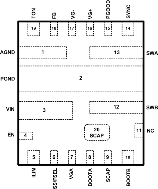
5 Pin Configuration and Functions
RNJ Package
VQFN (20 Pin)
Top View

Pin Functions
| PIN | I/O(1) | DESCRIPTION | |
|---|---|---|---|
| NAME | NO. | ||
| AGND | 1 | G | Analog signal ground of the IC. AGND should be connected to PGND and VG- at a single point on PCB (e.g. underneath the IC). |
| BOOTA | 8 | S | Bootstrap capacitor node for phase A high-side MOSFET gate driver. Connect the bootstrap capacitor from this pin to the SCAP pin (pin 9). |
| BOOTB | 10 | S | Bootstrap capacitor node for phase B high-side MOSFET gate driver. Connect the bootstrap capacitor from this pin to the SWB pin. |
| EN | 4 | I | Enable pin. Floating this pin will enable the IC. Pull below 1.23V to enter shutdown mode. Can also be used to adjust the input undervoltage lockout above 8 V with two resistors. |
| FB | 18 | I | Feedback pin for voltage regulation. Connect this pin to the center tap of a resistor divider to set the output voltage. |
| ILIM | 5 | I | Current limit programming pin. A resistor between this pin and ground sets the current limit. If no resistor is included, the default load current limit is 15 A. |
| NC | 11 | No connect. This pin is not electrically connected to the IC and is included for board level reliability (BLR) purposes. Connect this pin to the SCAP trace. | |
| PGND | 2 | G | Power ground of the IC. PGND should be connected to AGND and VG- at a single point on PCB (e.g. underneath the IC). Thermal vias to internal ground planes should be added beneath this pin. |
| PGOOD | 15 | O | Power good indicator. This pin is an open-drain output and will assert low if the output voltage is greater than ±5% away from the desired value or due to thermal shutdown, over-voltage/under-voltage, EN shutdown, or during soft start. A pull-up resistor can be connected between PGOOD and VG+ or an external logic supply pin. |
| SCAP | 9,20 | O | Series capacitor pin. Connect a ceramic capacitor from pin 20 to the SWA pin. |
| SS/FSEL | 6 | I | Soft start/frequency select pin. Connect a resistor from this pin to ground to set the soft-start time and the switching frequency. If no resistor is provided, the default setting of 4MHz oscillator frequency and 512µs soft start time is used. |
| SWA | 13 | O | Switching node for phase A. Connect an inductor from this pin to the output capacitors. |
| SWB | 12 | O | Switching node for phase B. Connect an inductor from this pin to the output capacitors. |
| SYNC | 14 | I | External clock synchronization pin. An external clock signal can be connected to this pin to synchronize the oscillator frequency (within ±10% of the nominal frequency set via SS/FSEL). |
| TON | 19 | I | On-time selection. An external resistor from this pin to the AGND pin programs the nominal on-time of the high side switches. |
| VG+ | 16 | S | Gate driver positive supply pin. Connect a bypass capacitor from this pin to VG-. To improve converter efficiency, the internal regulator can be overridden by connecting an external 5V supply to this pin. This supply rail also provides power to the control circuitry. |
| VG- | 17 | G | Gate driver supply return pin. VG- should be connected to PGND and AGND at a single point on PCB (e.g. underneath the IC). |
| VGA | 7 | S | High side phase A gate driver supply pin. Connect a bypass capacitor from this pin to ground. |
| VIN | 3 | I | The power input pin to the IC. Connect VIN to a supply voltage between 8 V and 14 V. |
(1) I = Input, O = Output, S = Supply, G = Ground Return