ZHCSEW7A December 2015 – April 2016 TPS54A20
PRODUCTION DATA.
- 1 特性
- 2 应用
- 3 说明
- 4 修订历史记录
- 5 Pin Configuration and Functions
- 6 Specifications
-
7 Detailed Description
- 7.1 Overview
- 7.2 Functional Block Diagram
- 7.3
Feature Description
- 7.3.1 Frequency Selection
- 7.3.2 External Clock Syncronization
- 7.3.3 Adjusting the Output Voltage
- 7.3.4 Soft Start
- 7.3.5 Startup into Pre-biased Outputs
- 7.3.6 Power Good (PGOOD)
- 7.3.7 Overcurrent Protection
- 7.3.8 Light Load Operation
- 7.3.9 Output Undervoltage/Overvoltage Protection
- 7.3.10 Input Undervoltage/Overvoltage Lockout
- 7.3.11 Enable and Adjusting Undervoltage Lockout
- 7.3.12 Series Capacitor Monitoring
- 7.3.13 Thermal Shutdown
- 7.3.14 Phase A Power Stage
- 7.3.15 Phase B Power Stage
- 7.3.16 Internal Gate Drive Regulator
- 7.3.17 Voltage Feed Forward
- 7.3.18 Internal Oscillator
- 7.3.19 Pulse Frequency Detector
- 7.3.20 On-Time Generator
-
8 Application and Implementation
- 8.1 Application Information
- 8.2
Typical Application
- 8.2.1 Design Requirements
- 8.2.2
Detailed Design Procedure
- 8.2.2.1 Output Voltage
- 8.2.2.2 Switching Frequency
- 8.2.2.3 On-Time
- 8.2.2.4 Inductor Selection
- 8.2.2.5 Output Capacitor Selection
- 8.2.2.6 Input Capacitor Selection
- 8.2.2.7 Series Capacitor Selection
- 8.2.2.8 Soft-Start Time Selection
- 8.2.2.9 Bootstrap Capacitor Selection
- 8.2.2.10 Gate Drive Capacitor Selection
- 8.2.2.11 Under Voltage Lockout Set Point
- 8.2.2.12 Current Limit Selection
- 8.2.3 Application Curves
- 9 Power Supply Recommendations
- 10Layout
- 11器件和文档支持
- 12机械、封装和可订购信息
6 Specifications
6.1 Absolute Maximum Ratings
over operating free-air temperature range (unless otherwise noted) (1)| MIN | MAX | UNIT | |||
|---|---|---|---|---|---|
| Input Voltage | Power Conversion, VIN | DC w.r.t. PGND, switching | –0.3 | 15 | V |
| DC w.r.t. PGND, non-switching | –0.3 | 17 | |||
| Bootstrap, V(BOOTA) | DC with respect to PGND | –0.3 | 22 | V | |
| DC with respect to SCAP | 6 | V | |||
| Bootstrap, V(BOOTB) | DC with respect to PGND | –0.3 | 14 | V | |
| DC with respect to SWB | 6 | V | |||
| Bias Supply, VG | DC with respect to PGND | –0.3 | 6 | V | |
| Series Capacitor Node Voltage, V(SCAP) | DC with respect to PGND | –0.3 | 16 | V | |
| Switch Node Voltage, V(SWA, SWB) | DC with respect to PGND | –1 | 9 | ||
| Pulse < 10 ns | –4 | 14 | |||
| Feedback, V(FB) | –0.3 | 3 | V | ||
| Output Voltage | Bias Supply, V(VGA) | DC with respect to PGND | –0.3 | 15 | V |
| Voltage | Enable Voltage, V(EN) | –0.3 | 7 | V | |
| Soft Start/Freq. Select, V(SS/FSEl) | –0.3 | 3 | |||
| Power Good Voltage, V(PGOOD) | –0.3 | 6 | |||
| External Sync Clock Voltage, V(SYNC) | –0.3 | 6 | |||
| Current Limit/Mode Select, V(ILIM) | –0.3 | 3 | |||
| On Time Pin Voltage, V(TON) | –0.3 | 3 | |||
| Input Current | Power Conversion, I(VIN) | 6 | A | ||
| Bias Supply, I(VG) | 100 | mA | |||
| Output Current | Switch Node A, I(SWA) | Current Limit | A | ||
| Switch Node B, I(SWB) | Current Limit | A | |||
| Operating Junction Temperature, TJ | –40 | 125 | °C | ||
| Storage temperature, Tstg | –65 | 150 | °C | ||
(1) Stresses beyond those listed under Absolute Maximum Ratings may cause permanent damage to the device. These are stress ratings only, which do not imply functional operation of the device at these or any other conditions beyond those indicated under Recommended Operating Conditions. Exposure to absolute-maximum-rated conditions for extended periods may affect device reliability.
6.2 ESD Ratings
| VALUE | UNIT | |||
|---|---|---|---|---|
| V(ESD) | Electrostatic discharge | Human body model (HBM), per ANSI/ESDA/JEDEC JS-001, all pins(1) | ±2000 | V |
| Charged device model (CDM), per JEDEC specification JESD22-C101, all pins(2) | ±500 | |||
(1) JEDEC document JEP155 states that 500-V HBM allows safe manufacturing with a standard ESD control process.
(2) JEDEC document JEP157 states that 250-V CDM allows safe manufacturing with a standard ESD control process.
6.3 Recommended Operating Conditions
over operating free-air temperature range (unless otherwise noted)| MIN | NOM | MAX | UNIT | ||
|---|---|---|---|---|---|
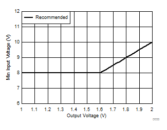
| VIN | Input Voltage | 8 | 14 | V | |
| VOUT | Output Voltage | 0.5 | VIN/5 | V | |
| IOUT | Output Current | 0 | 10 | A | |
| TJ | Junction Temperature | -40 | 125 | °C | |
6.4 Thermal Information
| THERMAL METRIC(1) | RNJ | UNIT | |
|---|---|---|---|
| 20 PINS | |||
| RθJA | Junction-to-ambient thermal resistance | 25(2) | °C/W |
| RθJC(top) | Junction-to-case (top) thermal resistance | 13.4 | °C/W |
| RθJB | Junction-to-board thermal resistance | 4.9 | °C/W |
| ψJT | Junction-to-top characterization parameter | 0.2 | °C/W |
| ψJB | Junction-to-board characterization parameter | 4.7 | °C/W |
| RθJC(bot) | Junction-to-case (bottom) thermal resistance | 2.0 | °C/W |
(1) For more information about traditional and new thermal metrics, see the IC Package Thermal Metrics application report, SPRA953.
(2) Tested on four layer evaluation board.
6.5 Electrical Characteristics
over operating free-air temperature range (unless otherwise noted)| PARAMETER | TEST CONDITIONS | MIN | TYP | MAX | UNIT | |
|---|---|---|---|---|---|---|
| SUPPLY VOLTAGE (VIN PIN) | ||||||
| VIN | VIN Operating | 8 | 12 | 14 | V | |
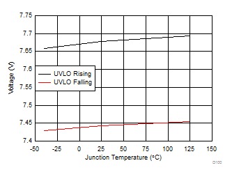
| VIN Input UVLO Voltage | VIN rising | 7.4 | 7.65 | 7.95 | V | |
| VIN UVLO hysteresis | 250 | mV | ||||
| VIN Input OVLO Voltage | VIN rising | 15.4 | 15.8 | V | ||
| VIN falling | 14.1 | 14.8 | V | |||
| VIN OVLO hysteresis | 600 | mV | ||||
| Shutdown | EN < 0.4 V, VIN = 12 V, TA = 25°C | 47 | µA | |||
| IQ | Operating into VIN | FB = 0.53 V, VIN = 12 V, TA = 25°C | 6 | mA | ||
| ENABLE (EN PIN) | ||||||
| Enable threshold | 1.17 | 1.23 | 1.27 | V | ||
| Input current | Enable threshold + 50 mV | –4 | µA | |||
| Enable threshold – 50 mV | –1 | µA | ||||
| VOLTAGE REFERENCE | ||||||
| Voltage Reference | TA = 25°C | 0.5054 | 0.508 | 0.5106 | V | |
| –40°C < TJ < 125°C | 0.5029 | 0.508 | 0.5131 | V | ||
| FREQUENCY | ||||||
| fOSC | Oscillator Frequency | R(SS/FSEL) = Open, 71.5 kΩ, or 48.7 kΩ |
3.6 | 4 | 4.4 | MHz |
| R(SS/FSEL) = Short or 35.7 kΩ | 6.3 | 7 | 7.7 | MHz | ||
| R(SS/FSEL) = 21.5 kΩ, 15.4 kΩ, or 8.66 kΩ |
9 | 10 | 11 | MHz | ||
| SYNC | ||||||
| Minimum Input Clock Pulsewidth | 20 | ns | ||||
| SYNC high threshold | 2 | V | ||||
| SYNC low threshold | 0.8 | V | ||||
| Frequency sync range | ±10 | % nominal | ||||
| Last SYNC falling/rising edge to return to resistor timing mode if SYNC is not present | 10 MHz: 400 ns 7 MHz: 571 ns 4 MHz : 1 µs |
4 | Cycles | |||
| LOW-SIDE A MOSFET | ||||||
| On resistance | VG = 5 V, Measured at pins | 6.8 | 10.5 | mΩ | ||
| LOW-SIDE B MOSFET | ||||||
| On resistance | VG = 5 V, Measured at pins | 9.3 | 14.8 | mΩ | ||
| HIGH-SIDE MOSFETS | ||||||
| On resistance | Vgs = 5 V, Measured at pins | 27 | 50 | mΩ | ||
| SW rise time 10% to 90% | VIN = 12 V | 2 | ns | |||
| SW fall time 90% to 10% | VIN = 12 V | 2 | ns | |||
| CURRENT LIMIT | ||||||
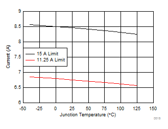
| Peak Switch LSA Current Limit | ~15A Load Trip, R(ILIM) = Open | 12.7 | 16.3 | 19.9 | A | |
| ~11.25A Load Trip, R(ILIM) = 47 kΩ | 9.9 | 12.7 | 15.5 | |||
| Peak Switch LSB Current Limit | ~15A Load Trip, R(ILIM) = Open | 6.8 | 8.7 | 10.6 | A | |
| ~11.25A Load Trip, R(ILIM) = 47 kΩ | 5.3 | 6.8 | 8.3 |
|||
| Overcurrent protection scheme | Hiccup | |||||
| OCP cycle count to trip fault | 3 | Cycles | ||||
| Fault hiccup wait time | 10 MHz: 13.1 ms 7 MHz: 18.7 ms 4 MHz: 32.8 ms |
131,072 | Cycles | |||
| INTERNAL REGULATOR (VG LDO) | ||||||
| Output Voltage | 0 mA ≤ IVG ≤ 100 mA | 4.4 | 4.8 | 5 | V | |
| Current Limit | 100 | 140 | mA | |||
| Nominal Operating Current | Fosc = 10 MHz, ILOAD = 10A | 60 | mA | |||
| DYNAMIC REGULATOR (VGA LDO) | ||||||
| Output Voltage | 15 | V | ||||
| VIN = 12 V | 10.5 | V | ||||
| SERIES CAP MONITOR | ||||||
| Low Voltage Fault Trip | 35 | 38 | %VIN | |||
| Nominal Voltage | 50 | |||||
| High Voltage Fault Trip | 62 | 65 | ||||
| Capacitor Precharge Current | 5.5 | 10 | 14.5 | mA | ||
| POWER GOOD | ||||||
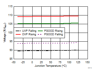
| VFB threshold | VFB falling (Fault), UVP | 90 | %VREF | |||
| VFB rising (Good) | 95 | |||||
| VFB rising (Fault), OVP | 110 | |||||
| VFB falling (Good) | 105 | |||||
| PGOOD sink current | V(PGOOD) = 0.4 V | 2.7 | mA | |||
| PGOOD pin leakage current | VFB = VREF, V(PGOOD)= 5 V | 1 | μA | |||
| Minimum VIN for valid PGOOD | V(PGOOD) ≤ 0.5 V at 100 µA | 1.2 | 2.75 | V | ||
| THERMAL SHUTDOWN | ||||||
| Thermal shutdown set threshold | 135 | °C | ||||
| Thermal shutdown hysteresis | 20 | °C | ||||
| Thermal shutdown hiccup time | 10 MHz: 13.1 ms 7 MHz: 18.7 ms 4 MHz: 32.8 ms |
131,072 | Cycles | |||
6.6 Timing Requirements
| MIN | NOM | MAX | UNIT | ||
|---|---|---|---|---|---|
| ENABLE (EN PIN) | |||||
| Enable to Start Switching time | 1 µF series cap, VIN = 12V | 625 | µs | ||
| SYNC | |||||
| Lock in time | 30 | µs | |||
| HIGH-SIDE MOSFETS | |||||
| SW minimum ON pulse width | 14 | ns | |||
| SW minimum OFF pulse width | 10 | ns | |||
| Non-Overlap Time between HS FET Off and LS FET On (deadtime) | Fsw = 5 MHz, VIN = 12 V | 3 | ns | ||
| Non-Overlap Time between LS FET Off and HS FET On (deadtime) | 3 | ns | |||
6.7 Typical Characteristics
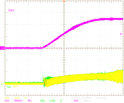
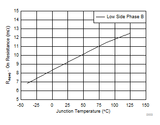
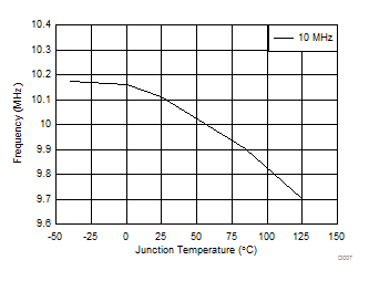
VIN = 12 V, VOUT = 1.2 V, TA = 25 ºC, unless otherwise noted.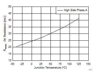

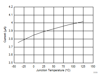
| EN = Threshold + 50 mV |

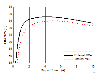
| fsw = 2 MHz per phase | 3.2 x 2.5 x 1.2 mm inductors |

| fsw = 2 MHz per phase | 3.2 x 2.5 x 1.2 mm inductors | No air flow |

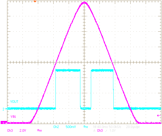
| 1 Ω Load | fsw = 2 MHz per phase | |
| 40 ms/div |
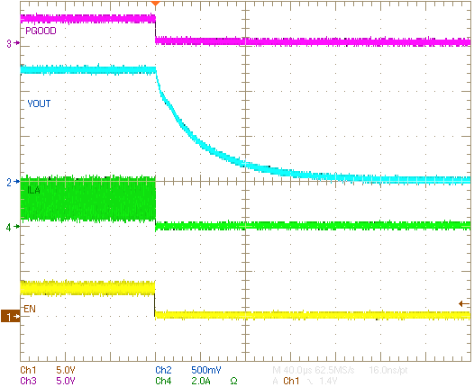
| 5 Ω Load | fsw = 2 MHz per phase | 40 µs/div |
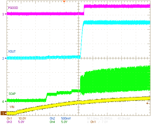
| Series capacitance = 1 µF | fsw = 2 MHz per phase | |
| 2 ms/div |
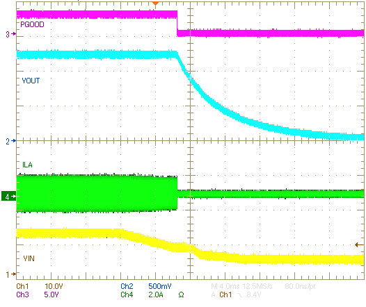
| 75 Ω Load | 4 ms/div |
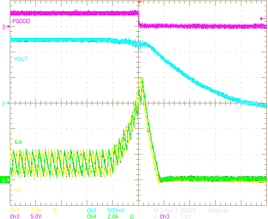
| fsw = 2 MHz per phase | 2 µs/div |
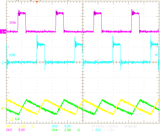
| fsw = 2 MHz per phase | 0 A load | 200 ns/div |
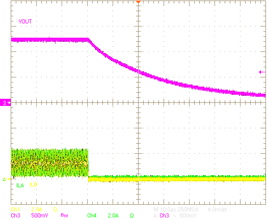

| Room temperature | 10 A load | No air flow |
| fsw = 2 MHz per phase | 3.2 x 2.5 x 1.2 mm inductors | Four layer board |

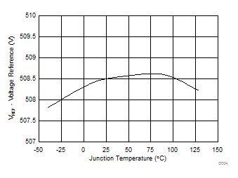
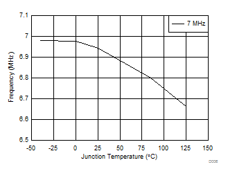
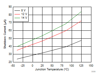
| EN = 0 V |
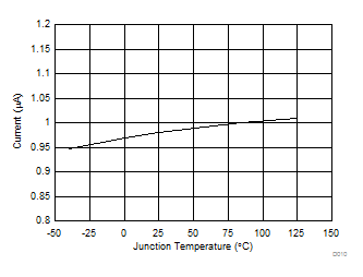
| EN = Threshold - 50 mV |
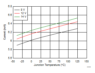
| FB = 0.53 V (non-switching) |
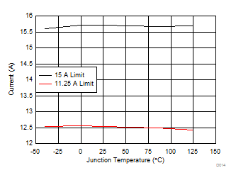
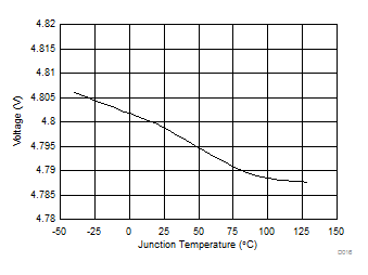

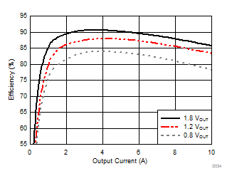
| fsw = 2 MHz per phase | External VG+ | 3.2 x 2.5 x 1.2 mm inductors |

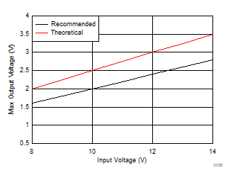

i.
Figure 26. Frequency vs Output Current
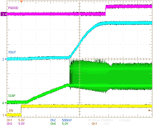
| Series capacitance = 1 µF | fsw = 2 MHz per phase | |
| 200 µs/div |
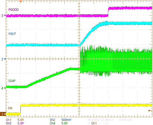
| Series capacitance = 1 µF | fsw = 2 MHz per phase | |
| 200 µs/div |
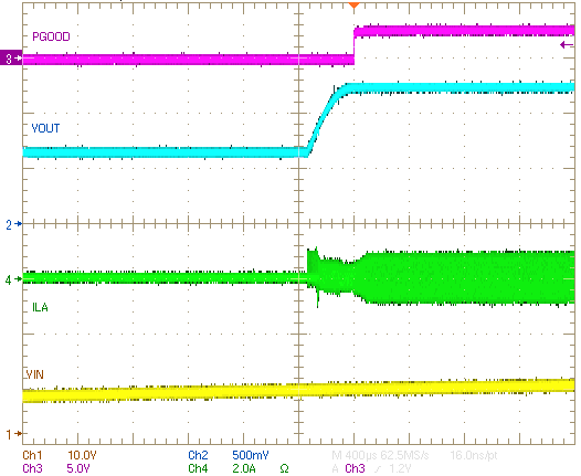
| 0 A Load | fsw = 2 MHz per phase | 400 µs/div |

| 0.5 Ω Load | 20 µs/div |

| 4 ms/div |
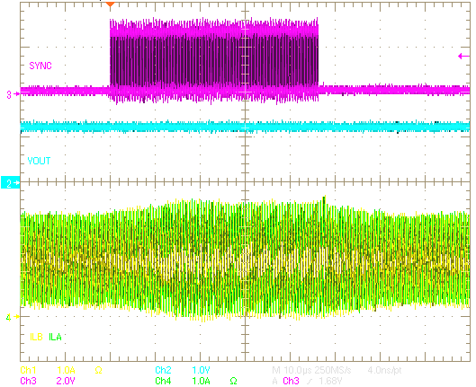
| 3.2 MHz SYNC clock |
